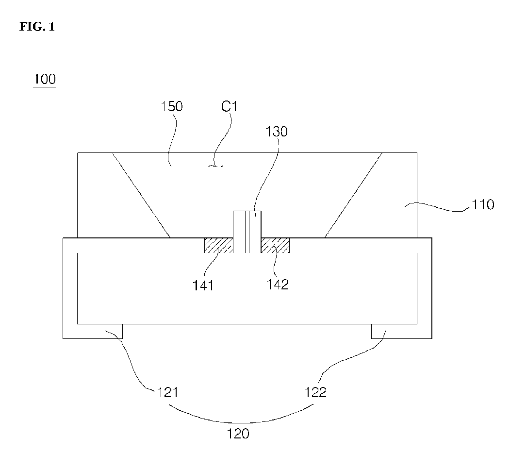
(57) Disclosed is a light emitting device package (100). The light emitting device package
(100) includes a body (110) provided with a cavity (C1), a first lead frame (121)
mounted on the body (110), a second lead frame (122) mounted on the body (110) and
separated from the first lead frame (121), and a light emitting device (130) mounted
in the cavity (C1) and disposed between the first lead frame and the second lead frame,
the light emitting device (130) is formed by sequentially stacking a first conductivity-type
semiconductor layer, an active layer and a second conductivity-type semiconductor
layer, the sequentially stacking direction of the first conductivity-type semiconductor
layer, the active layer and the second conductivity-type semiconductor layer is parallel
with the bottom surface of the cavity, the first lead frame (121) includes a first
connection part (141) electrically connected to the first conductivity-type semiconductor
layer, and the second lead (122) frame includes a second connection part (142) electrically
connected to the second conductivity-type semiconductor layer.
|
|
