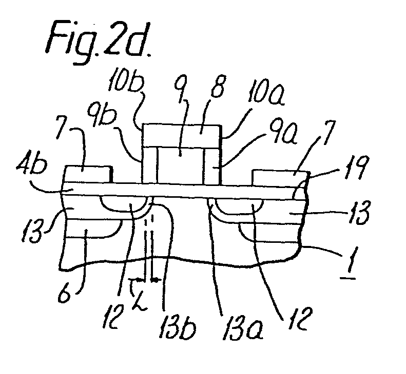
(57) A polycrystalline semiconductor layer (9) is provided on an insulating layer (4)
at the surface (19) of an n-type semiconductor body (1) and the gate of the IGFET
comprises strips (9a, 9b) which are formed by laterally diffusing a p-type impurity
into layer (9) below edges (10a, 10b) of masking layer (8). P-type zone (13) and the
n-type source (12) are formed by introducing the relevant impurities in the presence
of masking layer (8) and then by laterally diffusing these impurities below the gate,
zone (13) diffusing laterally further than source (12). Thus the lateral extent of
zone (12), source (13) and gate (9a, 9b) can all be predetermined in relation to the
same edge of masking layer (8) allowing improved gate-channel alignment and so minimizing
Miller capacitance of the IGFET.
|
|
