| (19) |
 |
|
(11) |
EP 0 090 738 B1 |
| (12) |
EUROPEAN PATENT SPECIFICATION |
| (45) |
Mention of the grant of the patent: |
|
12.07.1989 Bulletin 1989/28 |
| (22) |
Date of filing: 29.03.1983 |
|
| (51) |
International Patent Classification (IPC)4: H01L 27/02 |
|
| (54) |
Semiconductor device
Halbleiteranordnung
Dispositif semi-conducteur
|
| (84) |
Designated Contracting States: |
|
DE FR GB |
| (30) |
Priority: |
30.03.1982 JP 50079/82
|
| (43) |
Date of publication of application: |
|
05.10.1983 Bulletin 1983/40 |
| (73) |
Proprietor: FUJITSU LIMITED |
|
Kawasaki-shi,
Kanagawa 211 (JP) |
|
| (72) |
Inventors: |
|
- Enomoto, Hiromu
Kawasaki-shi
Kanagawa 210 (JP)
- Yasuda, Yasushi
Inagi-shi
Tokyo 206 (JP)
- Shimauchi, Yoshiki
Kawasaki-shi
Kanagawa 211 (JP)
- Tahara, Akinori
Zushi-shi
Kanagawa 249 (JP)
|
| (74) |
Representative: Descourtieux, Philippe et al |
|
Cabinet Beau de Loménie
158, rue de l'Université
75340 Paris Cédex 07
75340 Paris Cédex 07 (FR) |
| (56) |
References cited: :
EP-A- 0 029 717
US-A- 3 878 551
|
GB-A- 2 092 379
|
|
| |
|
|
- IBM TECHNICAL DISCLOSURE BULLETIN, vol. 21, no. 2, July 1978, pages 656-657, New York,
US; H.HEIMEIER et al.: "Integrated delay circuit"
- IBM TECHNICAL DISCLOSURE BULLETIN, vol. 14, no. 8, January 1972, page 2306, New York,
US; E.M.HUBACHER et al.: "Overvoltage protection in integrated circuits"
- IBM TECHNICAL DISCLOSURE BULLETIN, vol. 20, no. 10, March 1978, pages 3962-3963, New
York, US; O.ALAMEDDINE: "Protective circuit for integrated semiconductor devices"
- PATENTS ABSTRACTS OF JAPAN, vol. 7, no. 233 (E-204)[1378], 15th October 1983; & JP
- A - 58 121 663 (NIPPON DENKI K.K.) 20-07-1983
- PATENTS ABSTRACTS OF JAPAN, vol. 7, no. 170 (E-189)[1315], 27th July 1983; & JP -
A - 58 78 452 (TOKYO SHIBAURA DENKI K.K.) 12-05-1983
|
|
| |
|
| Note: Within nine months from the publication of the mention of the grant of the European
patent, any person may give notice to the European Patent Office of opposition to
the European patent
granted. Notice of opposition shall be filed in a written reasoned statement. It shall
not be deemed to
have been filed until the opposition fee has been paid. (Art. 99(1) European Patent
Convention).
|
Background of the invention
Field of the invention
[0001] The present invention relates to a logic circuit with parallel-connected Schottky
diodes connected to outer signal terminals.
Description of the prior art
[0002] It is known that input and/or output circuits are often electrostatically broken.
The applicants found that when a Schottky barrier diode formed by bringing an electrode
of metal such as aluminium into contact with an epitaxial layer is electrostatically
broken, aluminium of the elec- trade penetrates into the epitaxial layer and reaches
the underlying buried layer, resulting in a short circuit. A semiconductor device
provided with means for obtaining overvoltage protection in integrated circuits is
disclosed in IBM Technical Disclosure Bulletin Vol. 14, January 1972, page 2306, by
E. M. Hubacher et al A n
+ diffused buried region is provided along the boundary of a p-substrate and n-epitaxial
layer so as to form a pn
+ junction with a p-isolation diffusion region extending from the surface into the
p-substrate through the n-epitaxial layer. The isolation region is connected to a
voltage supply (-V) and the n-epitaxial layer to another voltage supply (-V). The
pn
+ junction serves as a clamp to protect the more sensitive junctions from power supply
overvoltage spikes.
Summary of the invention
[0003] An object of the present invention is to provide a logic circuit with parallel-connected
Schottky diodes, whose resistance against electrostatical breakage is improved.
[0004] This and other objects, features, and advantages of the invention are accomplished
by a logic circuit with parallel-connected Schottky diodes connected to outer signal
terminals, with each Schottky diode being formed by a structure comprising: a substrate;
an epitaxial layer of a first conductivity type formed on said substrate; a buried
impurity-doped region of the first conductivity type formed between said substrate
and said epitaxial layer; a first electrode formed on said epitaxial layer above said
buried impurity-doped region and electrically connected thereto; and a second electrode
formed on said epitaxial layer above said buried impurity-doped region to form a Schottky
barrier diode with said epitaxial layer, wherein at least one of said Schottky diodes
is protected by a structure comprising a second impurity-doped region of a second
conductivity type opposite to the first conductivity type, said second impurity-doped
region extending from a top surface of the epitaxial layer to said buried impurity-doped
region and being in contact with said buried impurity-doped region to form a pn junction
therewith, one of the buried impurity-doped region and second impurity-doped region
being electrically connected with the outer signal terminal which said protected Schottky
diode is connected to and the other one being electrically connected to a power source
terminal, whereby electrostatic breakage of said protected Schottky diode due to extraordinary
high voltage application from the outer signal terminal is prevented by preferential
breakdown of said pn junction.
[0005] In the semiconductor device according to the present invention, when a high potential
is applied to the buried region, the electrostatic charges stored in the buried region
flow through the second impurity-doped region by breakdown of the PN junction therebetween.
Thus, the PN junction prevents discharge between the buried layer and an electrode
of, e.g. aluminium, which would otherwise result in a short-circuit by penetration
of aluminium between them.
[0006] The second impurity-doped region may be preferably made by an element isolation region
in the semiconductor device.
Brief description of the drawings
[0007]
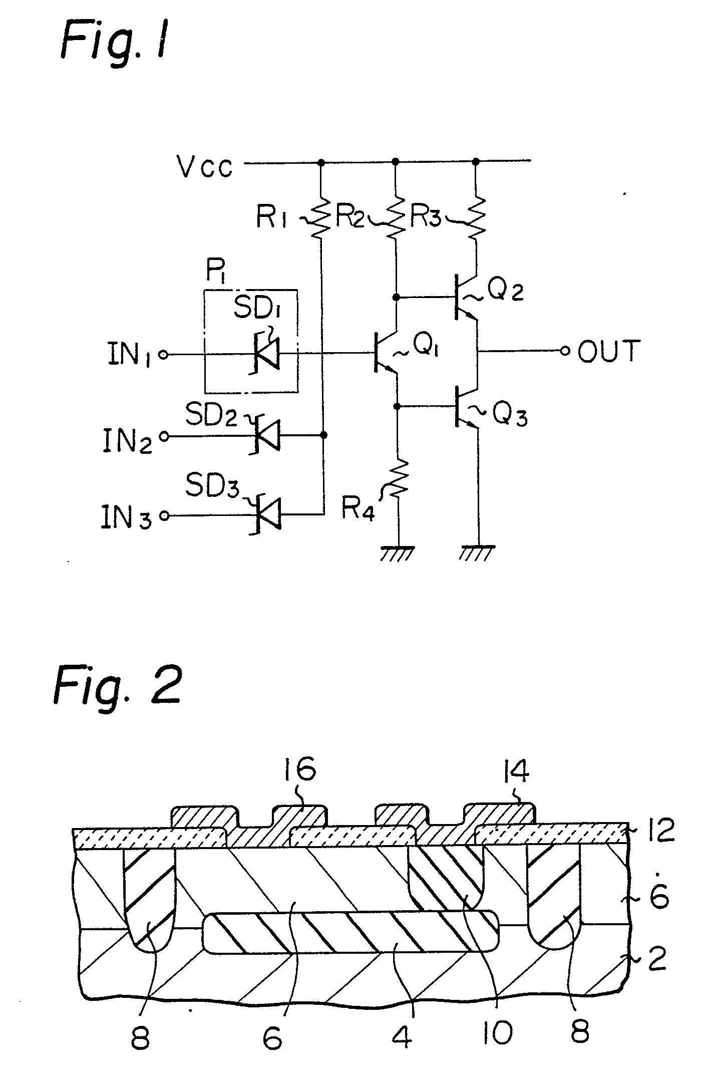
Figure 1 is a wiring diagram of a prior art transistor-transistor logic (TTL) circuit;
Figure 2 is a sectional view of a part of a semiconductor device including the TTL
circuit shown in Fig. 1;
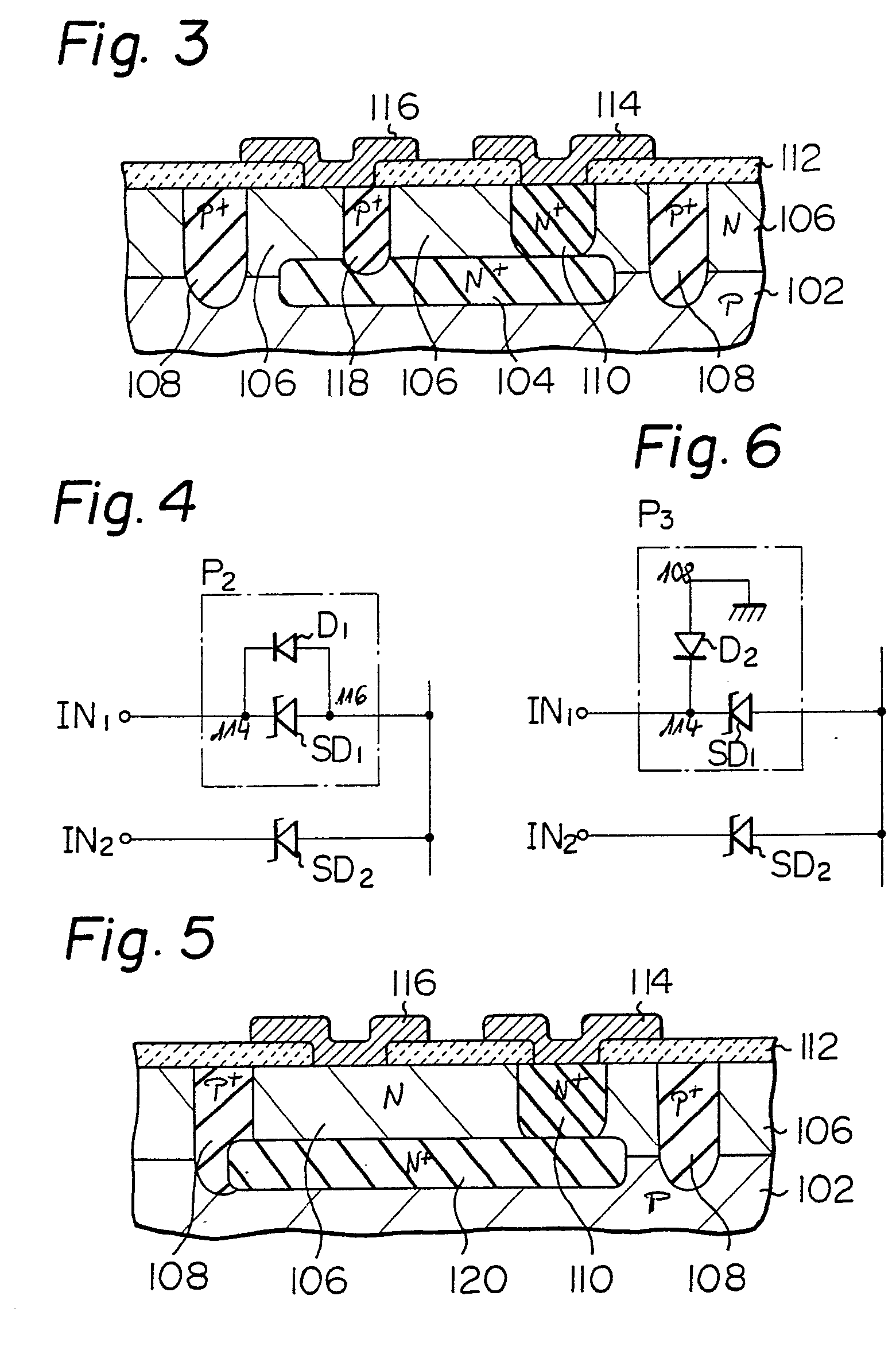
Figure 3 is a sectional view of a part of a circuit according to the present invention;
Figure 4 is a wiring diagram of the part shown in Fig. 3;
Figure 5 is a sectional view of a part of another circuit according to the present
invention, in which an impurity region is made by an isolation region; and
Figure 6 is a wiring diagram of the part shown in Fig. 5;
Description of the preferred embodiments
[0008] The present invention will now be described in detail in reference to prior art and
preferred embodiments.
Figure 1 is a wiring diagram of a prior art TTL circuit. Three Schottky diodes SD1, SD2, and SD3 are connected in parallel so as to form a three- input NAND gate at an input stage.
In the circuit, 01 is a phase dividing transistor, O2 and Q3 are transistors forming a push-pull output stage, R1, R2, R3, and R4 are resistors, and Vcc is a power source.
Figure 2 is a sectional view of a part P1 of a semiconductor device included in the prior art TTL circuit shown in Fig. 1,
the part P1 being enclosed by a broken line in Fig. 1. In a P-type silicon substrate 2, a buried
layer (N+b layer) 4 is formed by diffusion. An N-type epitaxial layer 6 is grown on the substrate
2, and an isolation region 8 and a contact region 10 for the buried layer 4 are formed
in the epitaxial layer 6 by P-type and N-type impurity diffusions respectively. In
many regions in the epitaxial layer 6, elements including input and/or output elements
are formed in accordance with a desired circuit. In Fig. 2, a Schottky barrier diode
SD1 is formed by bringing an electrode 16 of metal such as aluminum into contact with
the epitaxial layer 6. Reference numeral 12 denotes an insulating layer, and 14 and
16 electrodes.
Figure 3 is a sectional view of a part P2 of a semiconductor device according to the present invention. The semiconductor device
includes a TTL circuit similar to that shown in Fig. 1 exceptfor the part P1. The part P2 replaces the part P1.
[0009] Into a P-type silicon substrate 102, arsenic or antimony is selectively heat diffused
at about 1200°Cto 1300°Ctoform a buried layer (N
+b layer) 104. The buried layer 104 is about 3 µm (micrometer) in depth and about 20
Ω/□ in sheet resistance. On the substrate 102, an N-type silicon epitaxial layer 106
is grown. The epitaxial layer 106 is about 4 µm in thickness and about 0.6 to 0.9
Ω · cm in resistance. The surface of the epitaxial layer 106 is oxidised and patterned
to open windows for diffusion. These windows include not only windows for element
isolation, but also a window at a part of the area where a Schottky diode is later
formed. A boron silicate glass layer is formed entirely over the oxide layer. Then,
boron existing in the boron silicate glass is heat diffused at about 1200°C through
the windows to form isolation regions 108 as well as a boron-diffused region 118 reaching
the buried layer 104 under the window at a part of the area where the Schottky diode
is to be formed. These boron-diffused regions 108 and 118 are about 10
20 cm-
3 in boron concentration and about 6 Ω/□ in resistance. Then, according to a conventional
process, an N
+ contact region 110 is formed, an oxide layer 112 is formed and patterned, and an
aluminum layer is deposited and patterned to form electrodes 114 and 116 and conducting
lines (not shown).
[0010] The thus fabricated part P
2 shown in Fig. 3 corresponds to the enclosed part P
2 of the wiring diagram shown in Fig. 4. In Fig. 4, the PN junction formed by the contact
of the buried layer 104 and the boron-diffused region 118 is expressed by the diode
D
1.
[0011] In a semiconductor device according to the present invention, if an excessively high
electrostatic voltage is applied to an input terminal IN
1, the charge flows through the diode D
1, which has a breakdown voltage lower than the voltage at which electrostatic breakage
occurs between the buried layer 104 and the electrode 116, and through a resistor
R
1 or other parts to a power source or ground. Therefore, the Schottky barrier diode
SD
1 is not subject to excessive voltage, preventing electrostatic breakage.
[0012] To test the resistance against electrostatical breakage of the above fabricated semiconductor
device, electrostatic voltage was applied from a charged 200 pF capacitor with no
series connected resistance between the input terminal IN
1 connected with the electrode 114 and the ground connected with the boron-diffused
region 118. The resultant breakage voltage of the Schottky diode SD
1 was 230 V. For comparison, a semiconductor device of the prior art, similar to the
above semiconductor device except that the boron-diffused region 118 was not formed,
was also tested. The resultant voltage was 160 V.
[0013] Figure 5 illustrates another semiconductor device according to the present invention,
in which an impurity region corresponding to the boron-diffused region 118 in the
above example was formed by an element isolation region. In Fig. 5, 102 denotes a
silicon substrate, 106 an epitaxial layer, 108 an isolation region, 110 a contact
region, 112 an oxide layer, and 114 and 116 electrodes. This semiconductor device
was fabricated in the same manner as the above-described semiconductor device, except
that an arsenic- or antimony-diffused buried layer 120 was extended so as to have
a contact with the boron-diffused isolation region 108 and that no boron-diffused
region 118 extending from the electrode 112 to the buried layer 120 in the epitaxial
layer 106 was formed. Alternatively, a contact between an arsenic- or antimony-diffused
buried layer and a boron-diffused isolation region may be formed by extending the
isolation region not the buried layer or by combination thereof. The isolation region
108 having contact with the buried layer 120 is connected with the ground.
[0014] The part shown in Fig. 5 corresponds to the enclosed part P
3 of the wiring diagram of Fig. 6. The contact of the buried layer 120 and the isolation
region 108 is expressed as a diode D
2. The thus fabricated semiconductor device having a TTL circuit including the diode
D
2 was subjected to the same test as mentioned before. The resultant electrostatic breakage
voltage was 240 V.
1. A logic circuit with parallel-connected Schottky diodes (SDI, SD2, SD3) connected to outer signal terminals (IN1, IN2, IN3), with each Schottky diode being formed by a structure comprising: a substrate
(102; 202); an epitaxial layer (106) of a first conductivity type formed on said substrate;
a buried impurity-doped region (104; 120) ofthefirst conductivity type formed between
said substrate and said epitaxial layer; a first electrode (114) formed on said epitaxial
layer above said buried impurity-doped region and electrically connected thereto;
and a second electrode (116) formed on said epitaxial layer above said buried impurity-doped
region to form a Schottky barrier diode with said epitaxial layer, characterized in
that at least one (SD,) of said Schottky diodes is protected by a structure comprising
a second impurity-doped region (118; 108) of a second conductivity type opposite to
the first conductivity type, said second impurity-doped region extending from a top
surface of the epitaxial layer to said buried impurity-doped region (104; 120) and
being in contact with said buried impurity-doped region to form a pn junction therewith,
one of the buried impurity-doped region (104; 120) and second impurity-doped region
(118; 108) being electrically connected with the outer signal terminal (IN,) with
said protected Schottky diode (SDi) is connected to and the other one being electrically connected to a power source
terminal (Vcc or ground), whereby electrostatic breakage of said protected Schottky diode (SD1) due to extraordinary high voltage application from the outer signal terminal is
prevented by preferential breakdown of said pn junction.
2. A semiconductor device according to claim 1, characterized in that a third impurity-doped
region (110) of the first conductivity type extends from a top surface of the epitaxial
layer (106) to said buried impurity-doped region and is in contact with said electrode
(114) and said buried impurity-doped region.
3. A semiconductor device according to anyone of claims 1 to 3, characterized in that
said buried impurity-doped region (104; 120) is electrically connected with said outer
signal terminal (INI).
4. A semiconductor device according to any one of claims 1 to 3, characterized in
that said second impurity-doped region (118) is in contact with said second electrode
(116).
5. A semiconductor device according to any one of claims 1 to 4, characterized in
that it includes an element-isolating impurity-doped region (108) of a second conductivity
type, extending from a top surface of the epitaxial layer (106) into the substrate
(102) and defining a region of the epitaxial layer enclosed by said element-isolating
impurity-doped region as an element-forming region
6. A semiconductor device according to claim 5 characterized in that said element-isolating
impurity-doped region (108) constitutes said second impurity-doped region forming
a pn junction with said buried impurity-doped region (120).
1. Logikschaltung mit parallel verbundenen Schottky-Dioden (SD" SD2, SD3), die mit äußeren Signalanschlüssen (IN1, IN2, IN3) verbunden sind, wobei jede Schottky-Diode durch eine Struktur gebildet ist,
die umfaßt: ein Substrat (102; 202); eine epitaktische Schicht (106) von einem ersten
Leitfähigkeitstyp, die auf dem genannten Substrat gebildet ist; einen vergrabenen,
mit Verunreinigungen dotierten Bereich (104, 120) von dem ersten Leitfähigkeitstyp,
der zwischen dem genannten Substrat und der genannten epitaktischen Schicht gebildet
ist; eine erste Elektrode (114), die auf der genannten epitaktischen Schicht oberhalb
des genannten vergrabenen mit Verunreinigungen dotierten Bereiches gebildet und mit
diesem elektrisch verbunden ist; und eine zweite Elektrode (116), die auf der genannten
epitaktischen Schicht oberhalb des genannten vergrabenen, mit Verunreinigungen dotierten
Bereichs gebildet ist, um eine Schottky-Grenzschichtdiode mit der genannten epitaktischen
Schicht zu bilden, dadurch gekennzeichnet, daß wenigstens eine (SDi) der genannten Schottky-Dioden durch ein Struktur geschützt ist, welche einen zweiten
mit Verunreinigungen dotierten Bereich (118, 108) von einem zweiten Leitfähigkeitstyp,
entgegengesetzt zu dem ersten Leitfähigkeitstyp, umfaßt, welcher genannte zweite mit
Verunreinigungen dotierte Bereich sich von einer oberen Oberfläche der epitaktischen
Schicht zu dem genannten vergrabenen, mit Verunreinigungen dotierten Bereich (104;
120) erstreckt und mit dem genannten vergrabenen, mit Verunreinigungen dotierten Bereich
in Kontakt ist, um mit diesem einen pn-Übergang zu bilden, wobei ein vergrabener,
mit Verunreinigungen dotierter Bereich (104; 120) und der zweite mit Verunreinigungen
dotierte Bereich (118, 108) mit dem äußeren Signalanschluß (IN,) elektrisch verbunden
sind, mit dem die genannte geschützte Schottky-Diode (SDi) verbunden ist, und der andere elektrisch mit einem Energiequellenanschluß (Vcc oder Erde) verbunden ist, wodurch ein elektrostatischer Durchbruch der genannten
geschützten Schottky-Diode (SD1) aufgrund einer außerordentlich hohen Spannungsbeaufschlagung von dem äußeren Signalanschluß
durch vorzugsweisen Durchbruch des genannten pn-Übergangs verhindert wird.
2. Halbleitervorrichtung nach Anspruch 1, dadurch gekennzeichnet, daß ein dritter
mit Verunreinigungen dotierter Bereich (110) von dem ersten Leitfähigkeitstyp sich
von einer oberen Oberfläche der epitaktischen Schicht (106) zu dem genannten vergrabenen,
mit Verunreinigungen dotierten Bereich erstreckt und mit der genannten Elektrode (114)
und dem genannten vergrabenen, mit Verunreinigungen dotierten Bereich in Kontakt ist.
3. Vorrichtung nach einem der Ansprüche 1 bis 3, dadurch gekennzeichnet, daß der genannte,
mit Verunreinigungen dotierte Bereich (104; 120) mit dem genannten äußeren Signalanschluß
(INI) elektrisch verbunden ist.
4. Halbleitervorrichtung nach einem der Ansprüche 1 bis 3, dadurch gekennzeichnet,
daß der genannte zweite mit Verunreinigungen dotierte Bereich (118) mit der genannten
zweiten Elektrode (116) in Kontakt ist.
5. Halbleitervorrichtung nach einem der Ansprüche 1 bis 4, dadurch gekennzeichnet,
daß sie einen ein Element isolierenden, mit Verunreinigungen dotierten Bereich (108)
von einem zweiten Leitfähigkeitstyp umfaßt, der sich von einer oberen Oberfläche der
epitaktischen Schicht (106) in das Substrat (102) erstreckt und einen Bereich der
epitaktischen Schicht begrenzt, der durch den genannten elementisolierenden, mit Verunreinigungen
dotierten Bereich als einem elementbildenden Bereich eingeschlossen ist.
6. Halbleitervorrichtung nach Anspruch 5, dadurch gekennzeichnet, daß der genannte
elementisolierende, mit Verunreinigungen dotierte Bereich (108) den genannten zweiten
mit Verunreinigungen dotierten Bereich bildet, welcher einen pn-Übergang mit dem genannten
vergrabenen, mit Verunreinigungen dotierten Bereich (120) bildet.
1. Circuit logique doté de diodes de Schottky connectées en parallèle (SD,, SD2, SD3) qui sont connectées à des bornes de signaux extérieurs (IN1, IN2, IN3), chaque diode de Schottky étant formée par une structure comprenant: un substrat
(102; 202); une couche épitaxiale (106) d'un pre- miere type de conductivité formée
sur ledit substrat; une région enterrée dopée par des impuretés (104; 120) possédant
le premier type de conductivité et formée entre ledit substrat et ladite couche épitaxiale;
une première électrode (114) formée sur ladite couche épitaxiale au-dessus de ladite
région enterrée dopée par des impuretés et électriquement connectée à celle-ci; et
une deuxième électrode (116) formée sur ladite couche épitaxiale au-dessus de ladite
région enterrée dopée par des impuretés afin de former une diode à barrière de Schottky
avec ladite couche épitaxiale, caractérisé en ce qu'au moins une (SD,) desdites diodes
de Schottky est protégée par une structure comprenant une deuxième région dopée par
des impuretés (118; 108) possédant un deuxième type de conductivité opposé au premier
type de conductivité, ladite deuxième région dopée par des impuretés s'étendant de
la surface supérieure de la couche épitaxiale jusqu'à ladite région enterrée dopée
par des impuretés (104; 120) et étant en contact avec ladite région enterrée dopée
par des impuretés afin de former une jonction pn avec celle-ci, l'une des régions
que constituent la région enterrée dopée par des impuretés (104; 120) et la deuxième
région dopée par des impuretés (118; 108) étant électriquement connectée avec la borne
de signaux extérieurs (IN,) à laquelle ladite diode de Schottky (SD,) protégée est
connectée et l'autre étant électriquement connectée à une borne d'une source d'alimentation
(Vcc ou la terre), si bien que la rupture électrostatique de ladite diode de Schottky
(SD,) protégée qui serait provoquée par l'application d'une tension exceptionnellement
élevée en provenance de la borne de signaux extérieurs est empêchée parle claquage
préférentiel de ladite jonction pn.
2. Dispositif à semiconducteurs selon la revendication 1, caractérisé en ce qu'une
troisième région dopée par des impuretés (110) qui possède le premier type de conductivité
s'étend de la surface supérieure de la couche épitaxiale (106) jusqu'à ladite région
enterrée dopée par des impuretés et est en contact avec ladite électrode (114) et
ladite région enterrée dopée par des impuretés.
3. Dispositif à semiconducteurs selon l'une quelcpnque des revendications 1 à 3, caractérisé
en ce que ladite région enterrée dopée par des impuretés (104; 120) est électriquement
connectée à ladite borne de signaux extérieurs (INI).
4. Dispositif à semiconducteurs selon l'une quelconque des revendications 1 à 3, caractérisé
en ce que ladite deuxième région dopée par des impuretés (118) est en contact avec
ladite deuxième électrode (116).
5. Dispositif à semiconducteurs selon l'une quelconque des revendications 1 à 4, caractérisé
en ce qu'il comporte une région dopée par des impuretés d'isolation d'élément (108)
possédant un deuxième type de conductivité, qui s'étend de la surface supérieure de
la couche épitaxiale (106) jusque dans le substrat (102) et qui définit une région
de la couche épitaxiale entourée par ladite région dopée par des impuretés d'isolation
d'élément faisant fonction de région de formation d'élément.
6. Dispositif à semiconducteurs selon la revendication 5, caractérisé en ce que ladite
région dopée par des impuretés d'isolation d'élément (108) constitue ladite deuxième
région dopée par des impuretés formant une jonction pn avec ladite région enterrée
dopée par des impuretés (120).