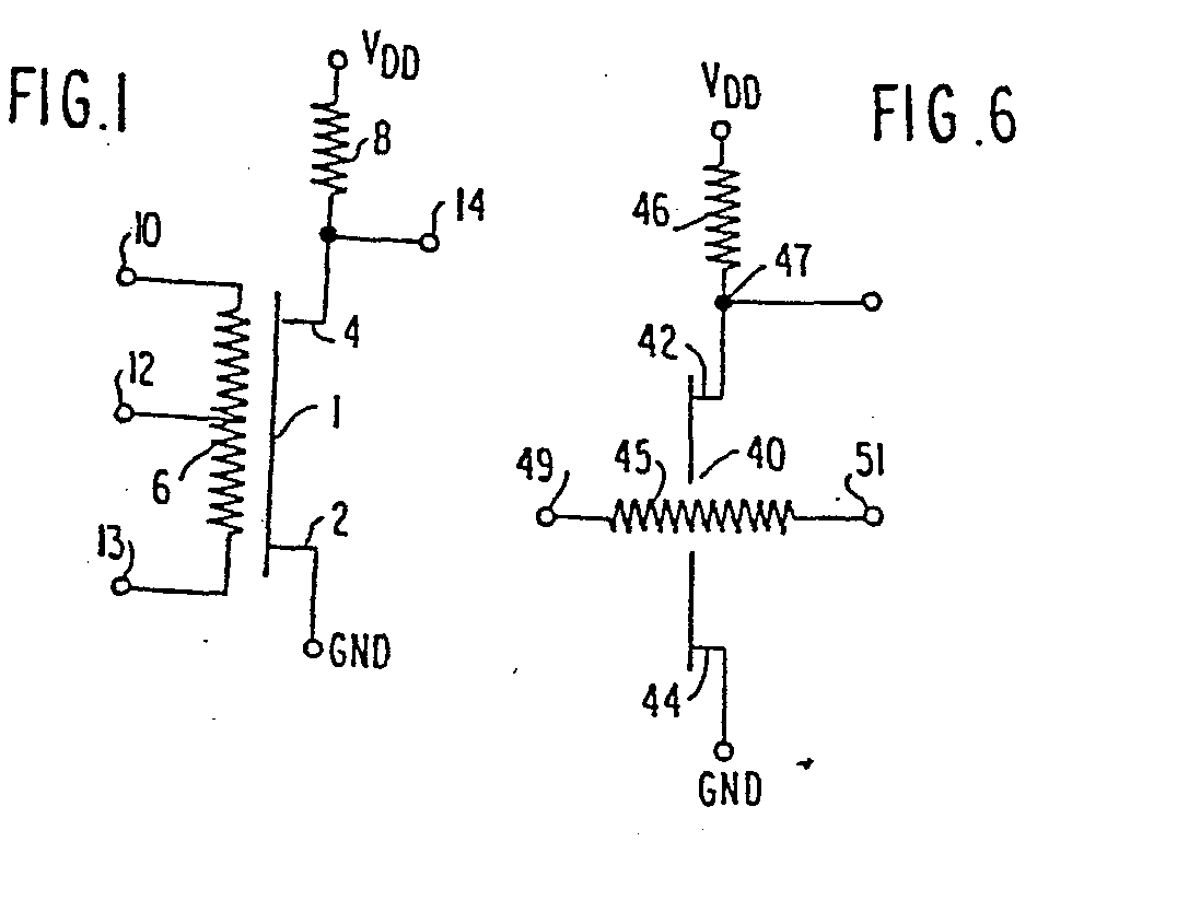
(57) @ A family of digital logic circuits constructed with resistive gate field effect
transistors is provided. The logic circuits are comprised of AND and OR circuits,
each implemented with resistive gate devices. In constructing an AND circuit (Figure
1 the resistive gate (6) lies along the length of the channel region between the source
(2) and drain (4) of the device. Logic input signals (at 10, 12, 13) are selectively
applied along the length of the channel region to the resistive gate. The device will
conduct between source and drain only if all points along the channel are above the
local threshold voltage of the channel region which will occur when appropriate logic
signals are applied simultaneously to all logic input terminals. A logic OR device
(Figure 6) is realized when the resistive gate (45) is formed transverse to the channel
such that each input to the gate controls a portion of the channel between the source
(44) and drain (42). NAND and NOR circuits are provided using the resistive gate logic
device in an inverting circuit context.
|
|
