| (19) |
 |
|
(11) |
EP 0 140 703 B1 |
| (12) |
EUROPEAN PATENT SPECIFICATION |
| (45) |
Mention of the grant of the patent: |
|
11.04.1990 Bulletin 1990/15 |
| (22) |
Date of filing: 30.10.1984 |
|
|
| (54) |
Pulse width decoder for double frequency encoded serial data
Pulsbreitendekoder für serielle, doppelfrequenzkodierte Daten
Décodeur de largeur d'impulsion pour données sérielles codées par fréquences doubles
|
| (84) |
Designated Contracting States: |
|
BE DE FR GB NL |
| (30) |
Priority: |
31.10.1983 US 547382
|
| (43) |
Date of publication of application: |
|
08.05.1985 Bulletin 1985/19 |
| (73) |
Proprietor: UNISYS CORPORATION |
|
Detroit
Michigan 48232 (US) |
|
| (72) |
Inventors: |
|
- Levy-Navarro, Bernardo
Ann Arbor
Michigan 48105 (US)
- Sylvernale, Ensi P.
West Chester, PA 19380 (US)
|
| (74) |
Representative: Webb, Frederick Ronald et al |
|
() |
| (56) |
References cited: :
WO-A-81/01226
|
US-A- 4 027 267
|
|
| |
|
|
- IBM TECHNICAL DISCLOSURE BULLETIN, vol. 21, no. 11, April 1979, pages 4611-4613, New
York, US; P.J. BROWN et al.: "Combinatorial diphase decoding"
|
|
| |
|
| Note: Within nine months from the publication of the mention of the grant of the European
patent, any person may give notice to the European Patent Office of opposition to
the European patent
granted. Notice of opposition shall be filed in a written reasoned statement. It shall
not be deemed to
have been filed until the opposition fee has been paid. (Art. 99(1) European Patent
Convention).
|
Background of the invention
[0001] Serial digital data is frequently transmitted using a self-clocking encoding. This
basic idea behind these self-clocking codes is to guarantee that a certain minimum
number of digital "events" (pulses or transitions in level) occur within the digital
waveform. These "guaranteed" events can then be used to establish and reconstruct
frequency and phase of the clocking signals which were used to encode and transmit
the data.
[0002] "Double frequency modulation" encoding is the simplest of the self-clocked encodings.
It is characterized by a guarantee that at least one, but no more than two digital
events occur per bit cell in the digital waveform. A bit cell is that portion of the
waveform which is generated by one cycle of the basic digital clock and contains a
single binary "0" or binary "1". The presence or absence of the second (non-guaranteed)
event depends upon the data being encoded.
[0003] Double frequency modulation (DFM) is referred to in the prior art as biphase-mark,
frequency modulation (FM), diphase, and frequency shift code (FSC).
[0004] A DFM encoded waveform contains pulses of two widths, long and short. A long pulse
is twice the width of a short pulse. Pulse width is defined as the time between two
transitions or edges. DFM waveforms alternate between positive and negative pulses.
[0005] The DFM encoding algorithm is quite simple. A sequence of two short adjacent pulses
of opposite polarity represents a logical "1" (or "mark"), while a long pulse of either
polarity represents a logical "0" (or "space"). DFM encoding may also be characterized
by the edges or transitions in the encoded waveform. A transition occurs at the start
of every bit cell. A "1" has an additional transition in the middle of the bit cell.
A "0" does not have any mid-cell transition. Another way of looking at the encoding
is that a "0" is encoded as a low frequency element, while a "1" is encoded as a high
frequency element; hence the name double frequency modulation.
[0006] Recovering data and clock information from a DFM waveform depends on the ability
to recognize the guaranteed transitions and to synchronize some timing circuit with
these recognized guaranteed transitions. The output of the timing circuit can then
be used, along with some additional logic, to extract data from the waveform. In the
prior art, various timing circuits have been used for this purpose. Two commonly used
techniques are briefly discussed below.
[0007] In the prior art technique, monostable multivibrators triggered by the guaranteed
transitions define a "window" during an interval when a non-guaranteed transition
may occur. The pulses produced by the monostables are then used to extract data from
the waveform. Technique 1 has the advantage of simplicity, but suffers from wide variations
in timing common with monostables. Further, technique 1 is quite susceptible to spurious
operation induced by noise in the incoming waveform and is limited to usage with relatively
low frequency signals.
[0008] In the second prior art technique, a variable frequency oscillator is synchronized
to the incoming frequency by means of a phase-locked loop. The output of the oscillator
is then used to extract data from the incoming waveform. Technique 2 eliminates the
timing tolerance problem associated with technique 1 and is much less prone to noise
induced failure. However, technique 2 is substantially more complex than technique
1. When working at high data rates (on the order of 100 Mb/s or higher) there can
be problems obtaining cost effective phase-locked loops that have the proper parameters.
In addition, a continuous bit stream of approximately forty or more bits is needed
to lock the phase-locked loop onto the desired frequency.
[0009] In certain applications where units containing circuits exemplified by techniques
1 to 2 are placed in series, such as in a ring network, the clocking signals derived
from the incoming waveform are used to construct an outgoing waveform for transmission
to the next unit downline. In such a configuration, "jitter" (viz., timing uncertainty)
in the output waveform must be minimized since the jitter may cascade and be amplified
by passage through several units in series. Phase-locked loops, such as those of technique
2, always exhibit frequency jitter. The amount of jitter is traded off against capture
time (time to go from initial "unlocked" state to "locked") and lock range (input
frequency range within which the phasq-locked loop will eventually enter the locked
condition). Since less jitter means less tracking ability and hence greater sensitivity
to component value tolerances, technique 2 may be unsuitable for applications in which
many units, each containing the extraction circuit, are cascaded in series. Using
technique 1 it is possible to design a circuit which exhibits no jitter beyond that
present in the incoming waveform, but one that suffers from the aforementioned drawbacks.
[0010] Previous efforts have been made to overcome the above discussed drawbacks of the
prior art. For example, in U.S. Patent Nos. 4,313,206 and 4,320,525, both of which
are assigned to the same assignee as the present invention, circuits are disclosed
for reconstructing the timing information encoded in a double frequency transition
event waveform. However, neither of these techniques provides for recovering the encoded
data information. In addition, these prior art techniques are designed to handle waveforms
having a frequency of 1 MHz. In contrast, some present and many planned communications
systems must be capable of operating at speeds exceeding 100 MHz.
[0011] The article by Brown et al "Combinatorial diphase decoding" in IBM Technical Disclosure
Bulletin, volume 21, No. 11, pages 4611-4613, discloses a decoder circuit in which
received signals are delayed by one half the basic repetition rate and inverted and
non-inverted versions of the delayed and undelayed signals are combined in four AND
gates, the outputs of two of which are applied to filter circuits to remove spurious
transients. The outputs of the filters are applied to a latch circuit which, when
set, enables further AND gates to derive data and clock signals.
[0012] WO-A-81-01226 discloses a decoder which generates three delayed versions of the incoming
double frequency encoded waveform. Transitions in the incoming waveform are detected
by comparing the waveform with the first delayed version and simultaneously comparing
the second and third delayed versions. The two generated transition waveforms are
used to from a composite clock which is used to toggle the state of a flip-flop at
one half bit intervals. The outputs of the flip-flop are gated with the first and
second
Jtransition waveforms to produce first and second clocking signals.
[0013] The present invention relates to a decoder circuit for deriving data and clock information
from an input double frequency encoded waveform, comprising: delay means, receiving
said input waveform, for producing delayed versions of said input waveform; data recovery
means for recovering the data information from said input waveform; and clock recovery
means for recovering the clock information from said input waveform.
[0014] The invention is characterised in that a first part of said recovery means is responsive
to said input waveform and a first one of said delayed versions to detect the occurrence
of a double high or a double low pulse in said input waveform, in that a second part
of said recovery means is responsive to the outputs of said first part and to said
first one of said delayed versions to remember whether a double low or a double high
preceded a pair of short pulses, in that a third part of said recovery means is responsive
to outputs of said first and second parts to provide said data information, and in
that a fourth part of said recovery means is responsive to said first and a second
one of said delayed versions and to the outputs of said first and second parts to
provide said clock information.
Brief description of the drawings
[0015]
Fig. 1 shows the double frequency modulation (DFM) waveform which enters the decoder
from the output of the receiver.
Fig. 2(A) shows a DFM waveform without pulse shortening effects. Fig. 2(B) shows a
DFM waveform . exhibiting pulse shortening.
Fig. 3 shows the receiver which provides the decoder with the DFM waveform and the
preferred embodiment of the decoder as implemented in ECL circuitry.
Fig. 4 is a timing diagram showing the raw DFM signals, R and R, the internal decoder
signals generated in response to the raw DFM signals, and the data and clock information
derived by the decoder for a double high (DH) "0" bit preceding "1" bits.
Fig. 5 is a timing diagram showing the raw DFM signals, R and R, the internal decoder
signals generated in response to the raw DFM signals, and the data and clock information
derived by the decoder for a double low (DL) "0" bit preceding "1" bits.
Detailed description of the preferred embodiment
[0016] The present pulse width decoder circuit derives NRZ-L data and clock information
from a double frequency encoded serial data bit stream. A double frequency modulation
(DFM) waveform (Fig. 1) drives the decoder DFM waveforms are well known in the prior
art, also being referred to as biphase-mark, frequency modulation (FM), diphase, or
frequency shift code (FSC) waveforms.
[0017] The DFM phase code is a self-clocking coding scheme in which clock and data information
are encoded together into one waveform. Referring to Fig. 1, it will be noted that
a DFM encoded waveform includes pulses of two widths, long and short. Pulse width
is defined as the time between two transitions or edges. A long pulse is twice the
width of a short pulse. DFM waveforms alternate between positive and negative pulses.
[0018] The encoding used in a DFM waveform is quite simple. A sequence of two short adjacent
pulses of opposite polarity is used to represent a logical "1" (or "mark"). A long
pulse of either polarity is used to represent a logical "0" (or "space"). DFM encoding
may also be characterized by the edges or transitions in the encoded waveform. Thus,
a transition occurs at the start of a bit cell. A logical "0" does not have any mid-cell
transition, whereas a logical "1" has a mid-cell transition.
[0019] Another way of characterizing DFM encoding is that a logical "0" is encoded as a
low frequency element, while a logical "1" is encoded as a high frequency element.
The latter mentioned characterization provides the basis for the name double frequency
modulation.
[0020] The present pulse width decoder circuit is driven by an inputted DFM waveform's rising
and falling edges. Data (D) and reconstructed clock (RCLK) information are output
by the decoder circuit. Basically, the present decoder circuit looks for long and
short pulses. A long pulse is decoded as a logical "0", while a pair of short, opposite
polarity pulses are decoded as a logical "1".
[0021] Additionally, the present decoder circuit decodes a short pulse followed by a long
pulse as a logical "1 ". This feature of the present decoder circuit allows the circuit
to tolerate pulse shortening in the DFM input waveform which may be caused by the
physical characteristics of the link circuits and/ortransmission medium. Fig. 2 shows
two DFM waveforms, one (Fig. 2(A)) being unaffected by pulse shortening and the other
(Fig. 2(B)) exhibiting pulse shortening. On wire links, saturation may cause shortening
of the first short pulse of a logical "1" bit that follows the long pulse of a logical
"0" bit. Although saturation will not occur in a glass fiber link, it is possible
for the transducer to create similar effects. The present decoder's ability to interpret
the short-long pulse sequence as a logical "1" allows the circuit to correctly decode
the affected data.
[0022] Fig. 3 shows the preferred embodiment of the present decoder circuit implemented
in ECL.
[0023] The preferred embodiment of the present invention (Fig. 3) was implemented using
the following components:
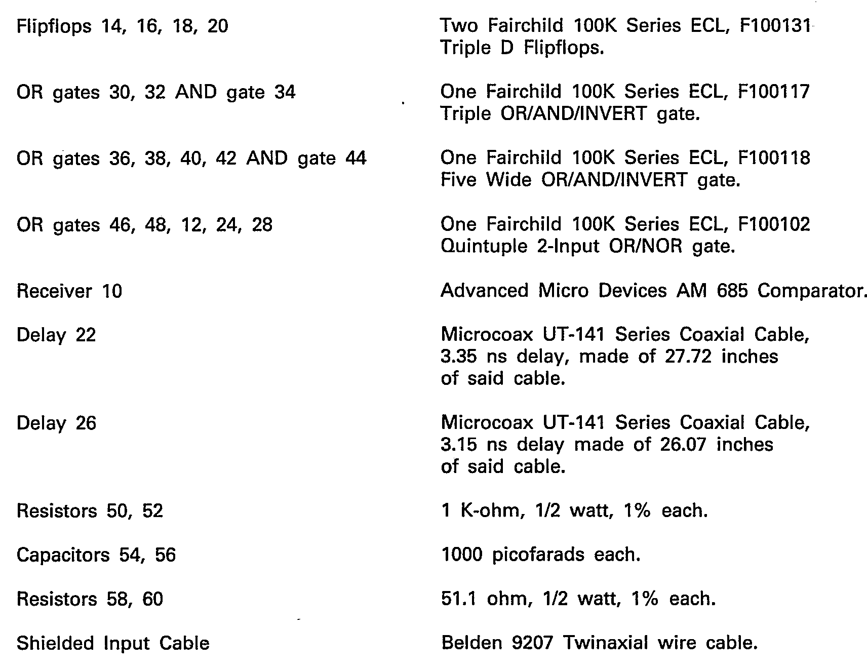
Those skilled in the art will appreciate that the preferred embodiment can readily
be implemented in other technologies such as Schottky TTL.
[0024] The raw DFM signal enters the decoder from the output of a receiver 10. In the preferred
embodiment, the receiver 10 is a high speed comparator which has its input capacitively
coupled to twinax cable. Those skilled in the art will appreciate that other types
of receivers and cables may be used, including fiber optic components. For purposes
of this discussion, suffice it to say that the raw DFM signal is provided at the output
of the receiver 10.
[0025] The raw DFM signal is fed through OR gate 12, the output of which provides inverted
and non-inverted signals R and R respectively, corresponding to the raw DFM signal.
The non-inverted DFM signal R clocks D-type flipflops 14, 16, and the inverted DFM
signal R clocks D-type flipflops 18 and 20.
[0026] The raw DFM signal output by receiver 10 is also fed into a first delay medium 22
which delays the raw DFM by approximately one third of a bit time. The delayed signals
from the first delay circuit 22 is fed through OR-gate 24 which provides inverted
and non-inverted versions A1 and Δ1 respectively of the first delayed DFM signal.
The first delayed versions Δ1 and Δ1 of the DFM signal are used to recover the clock
from the DFM waveform.
[0027] The first delayed version Δ1 of the DFM waveform output by delay medium 22 is further
delayed by delay medium 26 such that the waveform output by delay medium 26 represents
the raw DFM waveform delayed by approximately three quarters of a bit time. This second
delayed version of the raw DFM waveform is fed through OR gate 28 to create inverted
and non-inverted versions of the second delayed DFM waveform Δ2 and Δ2 respectively.
These second delayed versions A2 and A2 of the DFM waveform are used in the recovery
of both the data and clock information from the DFM waveform.
[0028] In the preferred embodiment, delay mediums 22 and 26 consist of specific lengths
of Microcoax coaxial cable, the lengths of the cable chosen to provide the desired
delay time. Those skilled in the art will appreciate that alternate means may be used
to achieve the desired delay of the raw DFM signal.
[0029] As previously mentioned, the present decoder looks for long pulses of either polarity.
Referring to Fig. 3 and the timing diagrams shown in Figs. 4 and 5, the DL flip-flop
14 looks for negative polarity long pulses (or "double low" (DL) pulses). The DH flip-flop
18 looks for positive polarity long pulses (or "double high" (DH) pulses).
[0030] The DL signal from flip-flop 14 thus goes high on the rising edge of the non-inverted
DFM signal R that marks the end of a DL pulse. The DL signal goes low on the rising
edge of the non-inverted DFM signal R that marks the middle or end of the first logical
"1" bit following the DL pulse. If pulse shortening prevents the DL signal from properly
going low, the next logical "1" bit will cause the DL signal to go low.
[0031] The DH signal from flip-flop 18 goes high on the falling edge of the non-inverted
DFM signal R at the end of a DH pulse. The DH signal goes low on the falling edge
of the non-inverted DFM signal R that marks the middle or end of the first logical
"1" bit following the DH pulse. If pulse shortening prevents the DH signal from properly
going low, the next logical "1" bit will cause the DH signal to go low.
[0032] The "double low last" (DLL) and "double high last" (DHL) flip-flops 16 and 20, respectively,
are used to remember which type of long pulse (logical "0" bit) preceded one or more
pairs of short pulses (logcal "1" bits). A DL pulse (from flip-flop 14) preceding
one or more logical "1" bits will cause the DLL flip-flop 16 to be set (via OR gate
48) since a DL pulse was the last long pulse before the logical "1" bit(s). The DLL
flip-flop 16 remains set due to the DLL signal being fed back through OR gate 48 until
it is reset by DH. Similarly, a DH pulse preceding one or more logical "1" bits will
cause the DHL flip-flop 20 to be set since a DH pulse was the last long pulse before
the logical "1" bit(s).
[0033] The DHL signal is set (via OR gate 46) on the falling edge of R when DH is high and
DL is low. DH thus acts as an asynchronous reset in this situation. The DHL flip-flop
20 remains set as long as logical "1"s continue to be input to the decoder. This is
accomplished by the DHL output of flip-flop 20 being fed back through OR gate 46 to
maintain flip-flop 20 in a set condition until it is reset by DL. The DHL flip-flop
20 is reset when the next logical "0" enters the decoder. DFM encoding again dictates
that this logical "0" must be a DL pulse since the preceding logical "0" was a DH
pulse. The DL pulse causes the DL signal to rise which resets DHL flip-flop 20.
[0034] To summarize, the DLL and DHL signals indicate the polarity of the last long pulse
(logical "0" bit) occurring before one or more pairs of short pulses (logical "1"
bit(s)). The DLL signal indicates that the last long pulse was low. The DHL signal
indicates that the last long pulse was high. If a series of logical "0" bits are input
to the decoder, both the DLL and DHL signals will remain low since DL and DH will
be continuously high.
[0035] When referring to the timing diagrams of Figs. 4 and 5, note that MR is used as an
abbreviation for the asynchronous master reset of flip-flop 16 or 20. Thus, MR=DL
means that the reset input R of DHL flip-flop 20 is connected to DL.
[0036] From the timing diagrams (Figs. 4 and 5), it can be seen that the decoder output
corresponds to DLL OR'ed with DHL. However, in fact one other operation must be performed
in order to complete the decoding of the data information from the DFM waveform. Thus,
if the present decoder is powered up such that the DL, DH, DLL and DHL signals are
all low and logical "1"s are input to the decoder, then the DL, DH, DLL and DHL signals
will remain low and the decoded outputs D and D will not reflect the encoded input.
To overcome this, a (DL · DH · DLL - DHL) term must be added to the calculation of
D. Thus,
[0037] 
[0038] Proper minimization of the above equation yields the OR-AND term to be used to implement
the decoder in ECL. Thus,

[0039] The above equation is implemented in the present decoder by OR-gate 30 which performs
an OR of DLL and DL, OR gate 32 which performs an OR of DHL and DH, and AND gate 34
which performs the logical AND of the outputs of OR gates 30 and 32 to provide the
receovered data bit D at its output.
[0040] The clock signal RCLK is derived from the A1 and Δ2 delayed versions of the DFM waveform
to create one clock edge every bit time. Depending on the polarity of the Δ1 and Δ2
waveforms, either (Δ1 · A2) or (A1 · Δ2) terms are used. Additional gating by DL,
DH, DLL and DHL allow formation of clock edges at the proper time. Thus, the clock
signal RCLK may be derived as follows:

Converting to OR-AND forms for the ECL implementation of the preferred embodiment,
we have

In the preferred embodiment, OR gate 36 is used to derive the term (DL+Δ1+Δ2), OR
GATE 38 is used to derive the term (DLL+Δ1 +Δ2), OR gate 40 is used to derive the
term (DH+AL +A2), and OR gate 42 is used to derive the term (DHL+Δ1+Δ2). The outputs
of OR gates 36, 38, 40 and 42 are combined in AND gate 44 to provide the recovered
clock signal RCLK.
[0041] Although the preferred embodiment of the present decoder circuit is implemented in
ECL, those skilled in the art will appreciate that the decoder can be implemented
in any technology that provides the basic logic device requirements of: D-flip-flops
with asynchronous reset, "OR" gates, "AND" gates, and delay elements which allow one-third
and three quarter bit time delays.
[0042] Having shown and described the preferred embodiment of the present invention, we
state that the subject matter which we regard as being our invention is particularly
pointed out and distinctly claimed in the following claims. Those skilled in the art
to which the present invention pertains will appreciate that equivalents or modifications
of, or substitutions for, parts of the specifically described embodiment of the invention
may be made without departing from the scope of of the invention as set forth in what
is claimed.
1. A decoder circuit for deriving data and clock information (D, D, RCLK, RCLK) from
an input double frequency encoded waveform (R), comprising: delay means (Δ1, A2),
receiving said input waveform, for producing delayed versions of said input waveform;
data recovery means (14, 16, 18, 20, 30, 32, 34) for recovering the data information
from said input waveform; and clock recovery means (14,16,18,20,36,38, 40,42) for
recovering the clock information from said input waveform, characterised in that a
first part (14, 18) of said recovery means is responsive to said input waveform (R)
and a first one of said delayed versions (A2) to detect the occurrence of a double
high (DH) or a double low (DL) pulse in said input waveform, in that a second part
(16, 20) of said recovery means is responsive to the outputs of said first part and
to said first one of said delayed versions to remember whether a double low or a double
high preceded a pair of short pulses, in that a third part (30, 32, 34) of said recovery
means is responsive to outputs of said first and second parts to provide said data
information (D, D), and in that a fourth part (36, 38, 40, 42) of said recovery means
is responsive to said first (A2) and a second one (Δ1) of said delayed versions and
to the outputs of said first and second parts to provide said clock information (RCLK,
RCLK).
2. A decoder circuit in accordance with Claim 1, wherein said second delayed version
(Δ1) of said input waveform corresponds to the input waveform delayed by approximately
one third of a bit time; and said first delayed version (A2) of said input waveform
corresponds to the input waveform delayed by approximately three quarters of said
bit time.
3. A decoder circuit in accordance with Claim 1 or Claim 2, wherein said first part
includes two D-type flip-flops, the first of which (18) detects the occurrence of
a double high and receives as its D input the first delayed version (A2) of said input
waveform and receives as its clock input the inverse (R) of the input waveform, and
the second of which (14) detects the occurrence of a double low and receives as its
D input the inverse of the first delayed version of said input waveform and receives
as its clock input the input waveform.
4. A decoder circuit in accordance with Claim 3, wherein said second part includes
two D-type flip-flops with asynchronous reset, the first of which (20) remembers whether
a double high preceded a pair of short pulses and receives as its D.input a signal
responsive to the Q output of the first flip-flop (18) included in said first part,
receives as its clock input the inverse of the input waveform, and receives as its
reset input the Q output of the second flip-flop (14) included in said first part;
and the second of which (16) remembers whether a double low preceded a pair of short
pulses and receives as its D input a signal responsive to the Q output of the second
flip-flop (14) included in said first part, receives as its clock input the input
waveform, and receives as its reset input the Q output of the first flip-flop (18)
included in said first part.
5. A decoder circuit in accordance with Claim 4, wherein the D input to the first
flip-flop (20) included in said second part is further responsive to its own Q output,
and the D input to the second flip-flop (16) included in said second part is further
responsive to its Q output.
6. A decoder circuit in accordance with Claim 4 or Claim 5, wherein said third part
includes a first logical OR gate (32) responsive to the Q output of the first flip-flop
(20) included in said second part and the Q output of the first flip-flop (18) included
in said first part; a second logical OR gate (30) responsive to the Q output of the
second flip-flop (16) included in said second part and the Q output of the second
flip-flop (14) included in said first part; and a first logical AND gate (34) responsive
to the output of said first and second logical OR gates, the output of said first
logical AND gate providing said recovered data information.
7. A decoder circuit in accordance with Claim 5 and Claim 6, wherein said second part
further includes a third logical OR gate (46) receiving as its inputs the Q outputs
of each of the first flip-flops included in said first and second part, the output
of said third logical OR gate providing the D input to the first flip-flop included
in said second part, and a fourth logical OR gate (48) receiving as its inputs the
Q outputs of each of the second flip-flops included in said first and second part,
the output of said fourth logical OR gate providing the D input to the second flip-flop
included in said second part.
8. A decoder circuit in accordance with any of Claims 4 to 7, wherein said fourth
part includes fifth (40) and sixth (42) logical OR gates, each receiving as inputs
the second delayed version (Δ1) of said input waveform and the inverse of the first
delayed version (A2) of said input waveform, said fifth logical OR gate (40) receiving
as a third input the Q output of the first flip-flop (18) included in said first part,
said sixth logical OR gate (42) receiving as a third input the Q output of the first
flip-flop (20) included in said second part; seventh (36) and an eighth (38) logical
OR gates, each receiving as inputs the first delayed version (A2) of the input waveform
and the inverse of the second delayed version (Δ1) of the input waveform, said seventh
logical OR gate (36) receiving as a third input the Q output of the second flip-flop
included in said first part, and said eighth logical OR gate (38) receiving as a third
input the Q output of the second flip-flop included in said second means; and a second
logical AND gate (44) receiving as its inputs and outputs of said fifth, sixth, seventh
and eighth logical OR gates, the output of said second logical AND gate providing
said clock information.
9. A decoder circuit in accordance with any of Claims 3 to 8, wherein each of said
flip-flops is triggered by a rising edge.
10. A decoder circuit in accordance with any of the preceding Claims, wherein said
second and first delayed versions are produced respectively by first and second delay
means (22, 26), each of which includes a section of microcoax coaxial cable.
11. A circuit wherein a decoder circuit in accordance with any of the preceding Claims
receives said input waveform from the output of a receiver (10), said receiver including
a high speed comparator which has its inputs capacitively coupled to a twinax cable.
12. A circuit in accordance with Claim 11, further including: a first logical OR/NOR
gate (12), responsive to the output of said receiver, the outputs of said first logical
OR/NOR gate providing inverted (R) and non-inverted (R) versions of said input waveform;
a second logical OR/NOR gate (24), responsive to the output of said first delay means
(22), the outputs of said second logical OR/NOR gate providing inverted and non-inverted
versions of the second delayed version of said input waveform; and a third logical
OR/NOR gate (28), responsive to the output of said second delay means, the outputs
of said third logical OR/NOR gate providing inverted and non-inverted versions of
the first delayed version of said input waveform.
1. Dekodierschaltung zum Gewinnen von Daten- und Taktinformationen (D, D, RCLK, RCLK)
aus einem doppelfrequenzkodierten Eingangssignal (R), die Verzögerungsmittel (A1,
A2) enthält, die das Eingangssignal empfangen und verzögerte Versionen dieses Eingangssignales
erzeugen, und die Daten - Rückgewinnungsmittel (14, 16, 18, 20, 30, 32, 34) zur Rückgewinnung
der Dateninformationen aus dem Eingangssignal und Takt - Rückgewinnungsmittel (14,
16, 18, 20, 36, 38, 40, 42) zur Rückgewinnung der Taktinformationen aus dem Eingangssignal
enthält, dadurch gekennzeichnet, daß ein erster Teil der Rückgewinnungsmittel (14,
18) auf das Eingangssignal (R) und auf ein erstes (A2) der verzögerten Eingangssignale
anspricht, um ein Auftreten von doppelten High-Impulsen (DH) oder doppelten Low-Impulsen
(DL) im Eingangssignal festzustellen; daß ein zweiter Teil (16,20) der Rückgewinnungsmittel
auf das Ausgangssignal des ersten Teils und auf das erste verzögerte Signal anspricht,
um festzuhalten, ob ein doppelt langer Low-Impuls oder ein doppelt langer High-Impuls
einem Paar von kurzen Pulsen vorausging; daß ein dritter Teil (30, 32, 34) der Rückgewinnungsmittel
auf die Ausgangssignale des ersten Teiles und des zweiten Teiles anspricht, um die
Dateninformationen (D, D) zur Verfügung zu stellen, und daß ein vierter Teil (36,
38, 40, 42) der Rückgewinnungsmittel auf das erste (A2) und ein zweites (A1) verzögertes
Eingangssignal sowie auf die Ausgangssignale des ersten Teils und des zweiten Teils
anspricht, um die Taktinformationen (RCLK, RCLK) zur Verfügung zu stellen.
2. Dekodierschaltung nach Anspruch 1, dadurch gekennzeichnet, daß das zweite verzögerte
Eingangssignal (A1) mit dem um annähernd ein Drittel der Bit-Dauer verzögerten Eingangssignal
übereinstimmt; daß das erste verzögerte Eingangssignal (A2) mit dem um annähernd dreiviertel
der Bit-Dauer verzögerten Eingangssignal übereinstimmt.
3. Dekodierschaltung nach Anspruch 1 oder 2, dadurch gekennzeichnet, daß der erste
Teil zwei D-Flipflops beinhaltet, deren erstes (18) das Vorkommen eines doppelten
High-Impulses feststellt, und an dessen D-Eingang das erste verzögerte Eingangssignal
(A2), und an dessen Takt-Eingang die Invertierung des Eingangssignals (R) anliegt;
deren zweites (14) das Vorkommen eines doppelten Low-Impulses feststellt, und an dessen
D-Eingang das invertierte erste verzögerte Eingangssignal und an dessen Takt-Eingang
das Eingangssignal anliegt.
4. Dekodierschaltung nach Anspruch 3, dadurch gekennzeichnet, daß der zweite Teil
zwei D-Flipflops mit asynchronem Reset beinhaltet, deren erstes (20) festhält, ob
ein doppelt langer High-Impuls einem Paar kurzer Impulse vorausging; dessen D-Eingang
auf den Q-Ausgang des ersten Flipflops (18) des ersten Teiles anspricht; an dessen
Takt-Eingang das invertierte Eingangssignal und an dessen Rücksetzeingang der Q-Ausgang
des zweiten Flipflops (14) des ersten Teiles anliegt; deren zweites (16) festhält,
ob ein doppelt langer Low-Impuls einem Paar kurzer Impulse vorausging und dessen D-Eingang
auf den Q-Ausgang des zweiten Flipflops (14) des ersten Teils anspricht; an dessen
Takt-Eingang das Eingangssignal und an dessen Rücksetzeingang der Q-Ausgang des ersten
Flipflops (18) des ersten Teils anliegt.
5. Dekodierschaltung nach Anspruch 4, dadurch gekennzeichnet, daß der D-Eingang des
ersten Flipflops (20) des zweiten Teiles zusätzlich auf seinen eigenen Q-Ausgang anspricht
und daß der D-Eingang des zweiten Flipflops (16) des zweiten Teiles zusätzlich auf
seinen eigenen Q-Ausgang anspricht.
6. Dekodierschaltung nach Anspruch 4 oder 5, dadurch gekennzeichnet, daß der dritte
Teile eine erste logische ODER-Verknüpfung (32) beinhaltet, die auf den Q-Ausgang
des ersten Flipflops (20) des zweiten Teiles und den Q-Ausgang des ersten Flipflops
(18) des ersten Teiles anspricht, und der eine zweite logische ODER-Verknüpfung (30)
beinhaltet, die auf den Q-Ausgang des zweiten Flipflops (16) des zweiten Teiles und
den Q-Ausgang des zweiten Flipflops (14) des ersten Teiles anspricht; der eine erste
logische UND-Verknüpfung (34) enthält, die auf die Ausgänge der ersten und der zweiten
logischen ODER-Verknüpfung anspricht, deren Ausgang die zurückgewonnenen Dateninformationen
zur Verfügung stellt.
7. Dekodierschaltung nach Anspruch 5 und 6, dadurch gekennzeichnet, daß der zweite
Teil zusätzlich eine dritte logische ODER-Verknüpfung (46) beinhaltet, an deren Eingängen
die Q-Ausgänge der jeweils ersten Flipflops des ersten und zweiten Teiles anliegen,
und dessen Ausgang am D-Eingang des ersten Flipflops des zweiten Teiles liegt; der
eine vierte logische ODER-Verknüpfung (48) beinhaltet, an deren Eingängen die Q-Ausgänge
der jeweils zweiten Flipflops des ersten und zweiten Teiles anliegen, und dessen Ausgang
am D-Eingang des zweiten Flipflops des zweiten Teiles liegt.
8. Dekodierschaltung nach einem der Ansprüche 4 bis 7, dadurch gekennzeichnet, daß
der vierte Teil eine fünfte (40) und sechste (42) logische ODER-Verknüpfung beinhaltet,
an deren Eingänge jeweils das zweite verzögerte Eingangssignal (Δ1) und die Invertierung
des ersten verzögerten Eingangssignals (A2) anliegen; daß an einem dritten Eingang
der fünften logischen ODER-Verknüpfung (40) der O-Ausgang des ersten Flipflops (18)
des ersten Teiles anliegt, und daß an einem dritten Eingang der sechsten logischen
ODER-Verknüpfung (42) der Q-Ausgang des ersten Flipflops (20) des zweiten Teiles anliegt;
daß der vierte Teil eine siebte (36) und achte (38) logischen ODER-Verknüpfung enthält,
an deren Eingängen jeweils das erste verzögerte Eingangssignal (A2) und die Invertierung
des zweiten verzögerten Eingangssignals (Δ1) anliegen; daß an einem dritten Eingang
der siebten logischen ODER-Verknüpfung (36) der Q-Ausgang des zweiten Flipflops des
ersten Teiles anliegt; daß an einem dritten Eingang der achten logischen ODER-Verknüpfung
(38) der Q-Ausgang des zweiten Flipflops des zweiten Teiles anliegt; daß an einer
zweiten logischen UND-Verknüpfung (44) an deren Eingängen die Ausgänge der fünften
(40), sechsten (42), siebten (36) und achten (38) logischen ODER-Verknüpfung anliegen;
daß der Ausgang der zweiten logischen UND-Verknüpfung (44) die Taktinformationen zur
Verfügung stellt.
9. Dekodierschaltung nach einem der Ansprüche 3 bis 8, dadurch gekennzeichnet, daß
jedes der Flipflops mit einer steigenden Flanke getriggert wird.
10. Dekodierschaltung nach einem der vorstehenden Ansprüche, dadurch gekennzeichnet,
daß das zweite und das erste verzögerte Eingangssignal von einem ersten und zweiten
Verzögerungsmittel (22, 26) erzeugt werden, von denen jedes ein Stück Microcoax-Koaxialkabel
enthält.
11. Schaltung mit einer Dekodierschaltung nach einem der vorstehenden Ansprüche, dadurch
gekennzeichnet, daß sie das Eingangssignal vom Ausgang eines Empfängers (10) erhält
und daß der Empfänger einen sehr schnellen Komparator enthält, dessen Eingänge kapazitiv
mit einem konzentrischen Kabel mit zwei Innenleitern gekoppelt sind.
12. Schaltung nach Anspruch 11, gekennzeichnet durch eine zusätzliche logische ODER/NICHT-ODER-Verknüpfung
(12), die auf den Ausgang des Empfängers anspricht und deren Ausgänge die Invertierung
des Eingangssignals (R) und das nicht-invertierte Eingangssignal (R) zur Verfügung
stellen; durch eine zweite zusätzliche logische ODER/NICHT-ODER-Verknüpfung (24),
die auf den Ausgang der ersten Verzögerungsleitung (22) anspricht und deren Ausgänge
das invertierte und das nicht-invertierte zweite verzögerte Eingangssignal zur Verfügung
stellen und durch eine zusätzliche dritte logische ODER/NICHT-ODER-Verknüpfung (28),
die auf den Ausgang der zweiten Verzögerungsmittel anspricht, und deren Ausgänge das
invertierte und das nicht-invertierte erste verzögerte Eingangssignal zur Verfügung
stellen.
1. Circuit-décodeur pour dériver des informations de données et d'horloge (D, D, RCLK,
RCLK) à partir d'une courbe d'entrée en codage à double fréquence (R), comportant
un moyen de temporisation (Al, A2) recevant la courbe d'entrée pour donner une version
retardée de cette courbe d'entrée, un moyen de récupération de données (14, 16, 18,
20, 30, 32, 34) pour récupérer l'information de données contenue dans la courbe d'entrée
et un moyen de récupération d'horloge (cadence) (14, 16, 18, 20, 36, 38, 40, 42) pour
récupérer l'information d'horloge contenue dans la courbe d'entrée, circuit caractérisé
en ce qu'une première partie (14, 18) du moyen de récupération est mise en oeuvre
par la courbe d'entrée (R) et une première version retardé (Δ2) pour détecter l'arrivée
d'une impulsion à double niveau haut ou double niveau bas (DH, DL) sous forme de courbe
d'entrée dans une seconde partie (16, 20) du moyen de récupération répond aux signaux
de sortie de la première partie et de la première des versions retardées pour rappeler
si un double niveau bas ou un double niveau haut a précédé une paire de courtes impulsions,
en ce qu'une troisième partie (30, 32, 34) de ce moyen de récupération est mise en
oeuvre par les sorties de la première et de la seconde partie pour fournir l'information
de données (D, D) et une quatrième partie (36, 38,40,42) du moyen de récupération
est mise en oeuvre par la première version retardée (A2) et la seconde version retardée
(Δ1) et les signaux de sortie de la première et de la seconde partie pour fournir
l'information d'horloge (RCLK, RCLK).
2. Circuit-décodeur selon la revendication 1, caractérisé en ce que la seconde version
retardée (Δ1) de la courbe d'entrée correspond à la courbe d'entrée retardée d'environ
un tiers de durée de bit et la première version retardée (A2) de la courbe d'entrée
correspond à la courbe d'entrée retardée d'environ trois-quart de durée de bit.
3. Circuit-décodeur selon la revendication 1 ou la revendication 2, caractérisé en
ce que la première partie se compose de deux flip-flop de type D dont le premier (18)
détecte l'arrivée d'un double niveau haut et reçoit sur son entrée D la première version
retardée (A2) de la courbe d'entrée et comme entrée d'horloge, l'inversion (R) de
la courbe d'entrée et le second (14) détecte l'arrivée d'un double niveau bas et reçoit
sur son entrée D l'inverse de la première version retardée de la courbe d'entrée,
et comme entrée d'horloge, la courbe d'entrée.
4. Circuit-décodeur selon la revendication 3, caractérisé en ce que la seconde partie
comprend deux flip-flop de type D avec remise à l'état initial asynchrone, le premier
(20) rappelant si un double niveau haut a précédé une paire de courtes impulsions
et recevant sur son entrée D un signal correspondant à la sortie Q du premier flip-flop
(18) appartenant à la première partie et comme entrée d'horloge l'inverse de la courbe
d'entrée et comme entrée de remise à l'état initial, la sortie Q du second flip-flop
(14) contenu dans la première partie et le second des flip-flop (16) rappelle si un
double niveau bas a précédé une paire de courtes impulsions, ce flip-flop recevant
sur son entrée D un signal correspondant à la sortie Q du second flip-flop (24) contenu
dans la première partie et sur son entrée d'horloge, la courbe d'entrée, et comme
entrée de remise à l'état initial, la sortie Q du premier flip-flop (18) apparenant
à la première partie.
5. Circuit-décodeur selon la revendication 4, caractérisé en ce que l'entrée D du
premier flip-flop (20) contenu dans la seconde partie répond en outre à sa propre
sortie Q et l'entrée D du second flip-flop (16) appartenant à la seconde partie répond
en outre à sa sortie Q.
6. Circuit-décodeur selon la revendication 4 ou la revendication 5, caractérisé en
ce que la troisième partie comporte une première porte OU logique (32) répondant à
la sortie Q du premier flip-flop (20) contenu dans la seconde partie et la sortie
Q du premier flip-flop (18) contenu dans la première partie; une seconde porte logique
OU (30) répondant à la sortie Q du second flip-flop (16) contenu dans la seconde partie
et la sortie Q du second flip-flop (14) contenu dans la première partie; et une première
porte logique ET (34) répondant à la sortie de la première et de la seconde porte
logique OU, la sortie de la première porte logique ET fournissant l'information de
données récupérée.
7. Circuit-décodeur selon la revendication 5 et la revendication 6, caractérisé en
ce que la seconde partie contient en outre une troisième porte logique OU (46) recevant
sur ses entrées les sorties Q de chacun des premiers flip-flop appartenant à la première
et à la seconde partie, la sortie de la troisième porte logique OU fournissant l'entrée
D au premier flip-flop appartenant à la seconde partie et une quatrième porte logique
OU (48) recevant sur son entrée les sorties Q de chacun des seconds flip-flop appartenant
à la première et à la seconde partie, la sortie de la quatrième porte logique OU fournissant
l'entrée D au second flip-flop appartenant à la seconde partie.
8. Circuit-décodeur selon l'une quelconque des revendications 4 à 7, caractérisé en
ce que la quatrième partie comporte une cinquième (40) et une sixième (42) porte logique
OU, chacune recevant en entrée la seconde version retardée (Δ1) de la courbe d'entrée
et l'inverse de la première version retardée (A2) de la courbe d'entrée, la cinquième
porte logique OU (40) recevant comme troisième entrée, la sortie Q du premier flip-flop
(18) appartenant à la première partie, la sixième porte logique OU (42) recevant comme
troisième entrée la sortie Q du premier flip-flop (20) contenu dans la seconde partie,
une septième (36) et une huitième (38) porte. logique OU, recevant chacune en entrée
la première version retardée (A2) de la courbe d'entrée et l'inverse de la seconde
version retardée (Δ1) de la courbe d'entrée, la septième porte logique OU (36) recevant
comme troisième entrée, la sortie Q du second flip-flop appartenant à la première
partie et la huitième porte logique OU (38) recevant comme troisième entrée, la sortie
Q du second flip-flop appartenant au second moyen; et une seconde porte logique ET
(44) recevant en entrée les signaux de sortie de la cinquième, sixième, septième et
huitième porte logique OU, la sortie de la seconde porte logique ET fournissant l'information
d'horloge.
9. Circuit-décodeur selon l'une quelconque des revendications 3 à 8, caractérisé en
ce que chacun des flip-flop est déclenché par un flanc montant.
10. Circuit-décodeur selon l'une quelconque des revendications précédentes, caractérisé
en ce que la seconde et la première version retardée sont fournies respectivement
par le premier et le second moyen de retard (22, 26) et chacun d'eux comporte une
longueur de câble coaxial microcoax.
11. Circuit comportant un circuit-décodeur selon l'une quelconque des revendications
1 à 10, caractérisé en ce qu'il reçoit une courbe d'entrée de la sortie du récepteur
(10), et ce récepteur comporte un comparateur travaillant à grande vitesse dont les
entrées sont couplées capacitivement sur un câble twinax.
12. Circuit selon la revendication 11, caractérisé en ce qu'il comprend en outre une
première porte logique OU/NOR (12) répondant à la sortie du récepteur, la sortie de
la première porte logique OU/NOR fournissant les versions inversée et non inversée
(R) et (R) de la courbe d'entrée; une seconde porte logique OU/NOR (24) répondant
à la sortie du premier moyen de retard (22), les sorties de la seconde porte logique
OU/NOR fournissant les versions inversée et non inversée de la seconde version retardée
de la courbe d'entrée et une troisième porte logique OU/NOR (28) répondant à la sortie
du second moyen de retard, les sorties de la troisième porte logique OU/NOR donnant
les versions inversée et non inversée de la première version retardée de la courbe
d'entrée.