| (19) |
 |
|
(11) |
EP 0 202 785 B1 |
| (12) |
EUROPEAN PATENT SPECIFICATION |
| (45) |
Mention of the grant of the patent: |
|
18.03.1992 Bulletin 1992/12 |
| (22) |
Date of filing: 23.04.1986 |
|
|
| (54) |
Nonvolatile electrically alterable memory
Nichtflüchtiger elektrisch änderbarer Speicher
Mémoire non-volatile altérable électriquement
|
| (84) |
Designated Contracting States: |
|
DE FR GB |
| (30) |
Priority: |
14.05.1985 US 734478
|
| (43) |
Date of publication of application: |
|
26.11.1986 Bulletin 1986/48 |
| (73) |
Proprietor: XICOR, INC |
|
Milpitas
California 95035 (US) |
|
| (72) |
Inventor: |
|
- Guterman, Daniel Charles
Fremont
California 94530 (US)
|
| (74) |
Representative: Cross, Rupert Edward Blount et al |
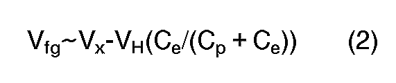
|
BOULT WADE TENNANT,
27 Furnival Street
London EC4A 1PQ
London EC4A 1PQ (GB) |
| (56) |
References cited: :
GB-A- 2 077 492
US-A- 4 486 769
|
US-A- 4 274 012
|
|
| |
|
|
- ELECTRONIC DESIGN, vol. 28, February 1980, no. 4, St. Rochelle Park; "Computer systems
acquire both RAM and EEPROM from one chip with two memories"
|
|
| |
|
| Note: Within nine months from the publication of the mention of the grant of the European
patent, any person may give notice to the European Patent Office of opposition to
the European patent
granted. Notice of opposition shall be filed in a written reasoned statement. It shall
not be deemed to
have been filed until the opposition fee has been paid. (Art. 99(1) European Patent
Convention).
|
[0001] The present invention relates generally to integrated circuit programmable nonvolatile
memory devices, and more particularly to an improved nonvolatile memory cell for increasing
the density of the nonvolatile memory cells in such memory devices.
Background of the Invention
[0002] In the prior art, integrated circuit memory devices have been developed which store
data for indefinite periods of time in the absence of electrical power being applied
thereto and which also have the capability of selectively changing or programming
the data stored therein. Of particular interest herein is a nonvolatile memory cell
which utilizes a floating gate as the nonvolatile element. See e.g., U.S. Patent No.
4,314,265 which discloses a four polysilicon layer, floating gate nonvolatile memory
cell, and U.S. Patent No. 4,274,012 which discloses a three polysilicon layer, floating
gate nonvolatile memory cell with substrate coupling. Either of these nonvolatile
memory cells may be arranged, as is known in the art, to construct nonvolatile random
access memories (NOVRAM's) and electrically erasable programmable read only memories
(EEPROM's). See, e.g., U.S. Patent No. 4,300,212, which discloses a NOVRAM device
and U.S. Patent No. 4,486,769, which discloses an EEPROM device. Of course, the principles
of the present invention are applicable to other devices utilizing floating gate technology.
[0003] In U.S. Patent No. 4,274,012, for example, the disclosed nonvolatile memory cell
has three layers of polysilicon, each layer being generally electrically isolated
from the substrate and each other. The first polysilicon layer is a programming electrode.
The second polysilicon layer is the floating gate. The floating gate has a portion
capacitively coupled to the programming electrode to form a programming tunneling
region in which electrons tunnel from the programming electrode to the floating gate.
Another portion of the floating gate is capacitively coupled to a n-implant region
in the p-type substrate. The n-implant region is a bias electrode. The third polysilicon
layer, which is an erase/store electrode, is capacitively coupled to a portion of
the floating gate to form an erase tunneling region in which electrons tunnel from
the floating gate to the erase/store electrode. Another portion of the erase/store
electrode is capacitively coupled to the bias electrode in the substrate.
[0004] To initiate tunneling, a high potential, such as 25v, is applied to the erase/store
electrode while the programming electrode is held at a low potential, such as ground.
The substrate bias electrode is caused to be held either at the low potential of the
programming electrode or held at the high potential of the erase/store electrode,
depending on whether electrons are to be tunneled from or to the floating gate, respectively.
With the bias electrode held at the high potential, the floating gate being strongly
capacitively coupled to the bias electrode is elevated to the high potential. Therefore,
high potential exists across the programming tunneling region between the programming
electrode and the floating gate so that electrons are tunneled onto the floating gate.
Conversely, with the bias electrode held at the low potential, the floating gate will
also be at the low potential because of the strong capacitive coupling to the bias
electrode. Therefore, high potential exists across the erase tunneling region between
the floating gate and the erase/store electrode. Electrons will then tunnel from the
floating gate to the erase/store electrode.
[0005] The above-described nonvolatile memory cell, in one useful application, forms the
nonvolatile portion of a NOVRAM memory cell disclosed in U.S. Patent No. 4,300,212.
The volatile portion of the NOVRAM memory cell is addressed, read from and written
to in a manner known for MOS flip-flop type memory cells. The nonvolatile portion
of the NOVRAM memory cell is coupled to the data and inverse data nodes of the volatile
portion of the NOVRAM memory cell. The bias electrode is connected to the drain of
an enhancement mode transistor with a grounded source. The data node of the volatile
portion of the NOVRAM memory cell is coupled to the gate of this transistor. When
the data node is at zero volts, representing one binary state, the transistor is turned
off allowing the bias electrode to be at a floating potential. The bias electrode
is further capacitively coupled to the erase/store electrode. Application of the high
voltage store pulse to the erase/store electrode will cause the potential of the bias
electrode to be elevated to the high potential. Electrons will then tunnel from the
programming electrode to the floating gate, as described hereinabove, giving it a
net negative charge. Conversely, when the data node is at 5 volts, representing the
other binary state, the transistor is turned on thereby coupling the bias electrode
to zero volts. Application of the high voltage pulse to the erase/store electrode
will cause electrons to be removed from the floating gate by tunneling to the erase/store
electrode, as described hereinabove, leaving a net positive charge thereon. Therefore,
the charge of the floating gate stores the state of the data node of the volatile
portion of the NOVRAM cell when the high voltage pulse is applied to the erase/store
electrode.
[0006] To sense the charge on the floating gate, the floating gate forms the gate of an
enhancement mode sense transistor. The drain of the sense transistor is coupled to
the inverse data node of the volatile portion of the NOVRAM memory cell. The sense
transistor is turned on when the floating gate has a net positive charge and is turned
off when the floating gate has a net negative charge. Thus, the charge stored on the
floating gate may be determined from the on or off state of the sense transistor and
the potential of the inverse data node set therefrom upon power up of the NOVRAM device.
[0007] The nonvolatile memory cell described in U.S. Patent No. 4,274,012, in another useful
application, is used in the construction of each memory cell in an array of cells
of an EEPROM device as disclosed in U.S. Patent No. 4,486,769. In the array disclosed
in this patent, the erase/store electrode is common to each cell in a column, and
the programming electrode is common to each cell in a row. Furthermore, the bias electrode
in each cell along a row are electrically connected to each other. To select one cell
in the array, the programming electrode across the row in which the selected cell
is located is held to a low potential, such as 0 volts and the erase/store electrode
of the column in which the selected cell is located is raised to a high potential,
such as 36 volts. The programming electrode in all other rows is raised to an intermediate
potential, such as 26 volts and the erase/store electrode in all other columns is
held to a low potential, such as 0 volts. The bias electrode for each cell in the
row of the selected cell is driven to either the intermediate potential or the low
potential, depending on whether the floating gate of the selected cell is to be programmed
or erased, respectively. The bias electrode for cells in all other rows is driven
to the intermediate potential. As described in the '769 patent, the full potential
difference between the low and high potentials will exist across either the programming
tunneling element or the erase tunneling element in the selected cell as a function
of the bias electrode potential. Electrons will then tunnel across the selected tunneling
element.
[0008] In all other cells along the row of the selected cell in this prior art EEPROM device,
a potential difference exists across the tunneling element between its programming
electrode and floating gate. The intermediate voltage applied to the bias electrode
of the unselected cell is partially coupled to the floating gate while the programming
electrode is held at the low potential. Since the unselected cell's erase/store electrode
is also held to zero volts, the capacitive coupling between the erase/store electrode
and the floating gate prevents the floating gate from having the same voltage as the
bias electrode. Thus, when the capacitive relationships are selected as describe in
the '769 patent, the floating gate in each of the cells in the row of the selected
cell will not have a potential sufficient to initiate tunneling of electrons to the
floating gate.
[0009] Similarly, a potential difference will exist across the tunneling region between
the erase/store electrode and floating gate of all other cells in the column of the
selected cell. Since the bias electrode and programming electrode of all nonselected
cells in this column are at the intermediate potential, their floating gates will
also have a potential near the intermediate potential. The erase/store electrode of
these selected cells in the column will be at the high potential. The resultant potential
difference across the erase tunneling region is therefore insufficient to cause elections
to tunnel from the floating gate.
[0010] In each cell of this EEPROM device, a pair of transistors are coupled to the channel
region of the substrate adjacent the floating gate. The gate of each of these transistors
is formed from the erase/store electrode. Data potential is coupled to the channel
region through one transistor and bias electrode potential is coupled to the channel
region through the other transistor. To erase the floating gate, both the data potential
and the bias electrode potential are at the low potential. To program the floating
gate, both the data potential and the bias electrode potential are at the intermediate
potential.
[0011] The above approach has several limitations. First, a number of capacitance interrelationships
and tunnel voltage requirements must be maintained in order to avoid data disturbs
of unselected cells during a write operation. In addition, logistical requirements
of arrayed cells can make a single cycle write operation difficult to implement in
practice. Consequently, in practical operation, before the floating gate is programmed,
each EEPROM cell is first erased. Thus, each write cycle to a memory cell is preceded
by an unconditional erase cycle, incurring unnecessary write time and cell wear out.
[0012] It is desirable to increase the number of memory devices which are fabricated from
a single wafer to increase the chip yield per wafer and thereby to reduce the cost
of each chip. In this regard, the size of each memory cell within the memory device
must be reduced. However, such reductions in size do not allow a simple miniaturization
of existing memory cells. For example, tolerances between mask levels may be difficult
to maintain or the miniaturized design may require minimum channel widths not compatible
with existing technology. Miniaturization of the above-described nonvolatile memory
cell does not allow the necessary capacitive values and relationships to be maintained
for an operational memory device. For example, should the required capacitive relationships
in the EEPROM device described in the '769 patent not be maintained, the voltages
described as occurring across the tunneling regions of unselected cells in the row
and columns of the selected cell may be sufficient to cause inadvertent tunneling
or a data disturb of the unselected cell. Furthermore, the overhead requirements of
a separate and distinct bias electrode region for a write operation, and floating
gate channel region for a read operation, combined with the aforementioned inherent
tolerance requirements needed to prevent disturb conditions, makes shrinking of present
memory cells for very high density applications impractical.
[0013] It is also desirable to eliminate one or more of the above-described capacitive couplings
in the NOVRAM device. Such capacitive couplings introduce losses in obtaining the
voltage relationships necessary to induce tunneling of electrons between the polysilicon
layers. Eliminating such capacitors, therefore, would improve device operation. Furthermore,
the elimination of these capacitances enables a greater degree of miniaturization,
since the need for the large amount of chip real estate required to form such capacitors
would be eliminated.
[0014] Furthermore, device operation and cell dimensions could be optimized by reducing
component count in each memory cell and reducing the number of cycles required for
a write operation. For example, in the EEPROM device, it is desirable that a write
cycle (programming the floating gate) be accomplished in a single cycle obviating
the need for an unconditional erase prior to each write cycle.
[0015] The present invention provides a nonvolatile floating gate device comprising a substrate
of a first conductivity type having a first surface and a first substrate region disposed
in said first surface, said first substrate region being of a second conductivity
type opposite said first conductivity type; first means for selectively applying one
of a first data potential and a second data potential to said first substrate region,
said first data potential being applied when data to be stored in said device has
one binary state, said second data potential being applied when data to be stored
in said device has the other binary state; a first electrically insulated semiconductor
layer; second means for applying a first bias potential to said first semiconductor
layer; a second electrically insulated semiconductor layer being a floating gate having
a first portion capacitively coupled to said first layer and a second portion capacitively
coupled to a portion of said first surface; a third electrically insulated semiconductor
layer having a first portion capacitively coupled to said second portion of said second
semiconductor layer and a second portion being capacitively coupled to said first
surface and adjacent an edge of said first substrate region, said second portion of
said third semiconductor layer being disposed generally intermediate said first substrate
region and said second portion of said second semiconductor layer; third means for
selectively applying a first control potential to said third semiconductor layer,
said control potential being selected to invert the conductivity type of said first
surface capacitively coupled to said second portion of said third semiconductor layer
to said second conductivity type to electrically couple the potential of said first
region to a portion of said surface of said substrate capacitively coupled to said
second portion of said second semiconductor layer, each said potential being selected
so that electrons are introduced onto said second semiconductor layer from said first
semiconductor layer upon application of the first data potential to said first substrate
region and said control potential to said third semiconductor layer, and further selected
so that electrons are removed from said second semiconductor layer to said third semiconductor
layer upon application of said second data potential to said first substrate region
and said control potential to said third semiconductor layer; and means for sensing
the potential of said floating gate.
[0016] The present invention also provides a nonvolatile floating gate device comprising
a substrate of a first conductivity type having a first surface; a first electrically
insulated semiconductor layer being spaced from said first surface; first means for
applying a bias potential to said first semiconductor layer; an electrically insulated
semiconductor floating gate having a first portion and a second portion, said first
portion being capacitively coupled to said first semiconductor layer; a first transistor
having a first gate, a source and a drain, said first transistor for selectively coupling
the potential of one of said source and drain to said floating gate; second means
for selectively applying one of a first data potential and a second data potential
to said one of said source and said drain, said first data potential being applied
when data to be stored in said device has one binary state, said second data potential
being applied when data to be stored in said device has the other binary state; third
means for selectively applying a first control potential to said first gate, said
control potential being selected to turn said first transistor on, each said potential
being selected so that electrons are introduced onto said floating gate from said
first semiconductor layer upon application of said first data potential to said one
of said source and said drain when said transistor is turned on by said control potential,
and further so that electrons are removed from said floating gate to said first gate
of said first transistor upon application of said second data potential to said one
of said source and said drain when said transistor is turned on; and means for sensing
the potential of said floating gate.
[0017] The present invention further provides an integrated circuit memory device having
a plurality of nonvolatile memory cells interconnected into an array having a plurality
of rows and a plurality of columns, said device comprising a semiconductor substrate
of a first conductivity type having a first surface, in which said memory cells are
disposed, a plurality of first substrate regions and a second substrate region, each
of said substrate regions being of a second conductivity type opposite said first
conductivity type, each of said first substrate regions being disposed within a portion
of said cells along an associated one of said columns, said second substrate region
being disposed within a portion of all of said cells; first means for applying a reference
potential to said second substrate region; second means for selectively applying one
of a first data potential representing a first binary data state and a second data
potential representing a second binary data state to selected ones of said first substrate
regions; a first electrically insulated semiconductor layer spaced from said first
surface and overlying a portion of each of said cells forming a first channel region
in said first surface in each of said cells, each said first channel region being
adjacent a portion of said second substrate region within the associated one of said
cells; third means for applying a first bias potential to said first semiconductor
layer, said bias potential and said reference potential being selected to electrically
isolate said first channel region in each of said cells from said second substrate
region; a plurality of second electrically insulated semiconductor layers, each of
said second semiconductor layers being associated with one of said cells and having
a first portion capacitively coupled to a portion of said first semicondcutor layer
within said associated one of said cells and a second portion overlying a portion
of said substrate in said associated one of said cells; a plurality of third electrically
insulated semicondcutor layers spaced from said first surface, each of said third
semiconductor layers being associated with one of said rows and overlying a portion
of each of said cells in the associated one of said rows and having a plurality of
first portions and a plurality of second portions, each of said first portions of
said third semiconductor layer being capacitively coupled to an associated one of
said second semiconductor layers, each of said second portions of said third semiconductor
layer overlying a portion of said substrate in the associated one of said cells forming
a second channel region in each of said cells, said second channel region in each
one of said cells being intermediate a portion of one of said first substrate regions
associated with said one of said cells and said portion of said substrate in said
one of said cells; fourth means for selectively applying a first control potential
to the third semiconductor layers of a selected one of said rows, said control potential
being selected to invert the conductivity type of said second channel region to said
second conductivity type to electrically couple the potential of one of said first
substrate regions associated with each of said cells in said selected row to said
portion of said substrate, each said potential being selected so that electrons are
introduced onto said second semiconductor layer in each of said cells along said selected
row from said first semiconductor layer when said first data potential is applied
to said associated one of said first substrate regions and so that electrons are removed
from said second semiconductor layer to one of said third semicondcutor layers associated
with said one of said cells when said second data potential is applied to the associated
one of said first substrate regions; and means for sensing the potential of each of
said second semiconductor layers.
[0018] Thus the present invention can provide a nonvolatile memory cell which is smaller
than known nonvolatile memory cells and which utilises fewer components than known
memory cells.
[0019] The present invention can also provide a nonvolatile memory cell which eliminates
some capacitive relationships, thereby minimising the chip real estate required for
forming such cells, since less overlap between layers of the memory cell is required.
[0020] The present invention can further provide a nonvolatile memory cell which obviates
the requirement of an unconditional erase cycle prior to programming the floating
gate.
[0021] The present invention can still further provide a dense nonvolatile integrated circuit
memory device which substantially eliminates data disturb conditions in unselected
cells of the memory device when writing into one or more selected cells.
[0022] The nonvolatile memory cell of one aspect of the present invention includes three
electrically isolated semiconductor layers, generally as described hereinabove. That
is, the first layer forms the programming electrode, the second layer forms the floating
gate, and the third layer forms the erase/store electrode.
[0023] Embodiments of the present invention eliminate the need for capacitive coupling between
the third semiconductor layer, the erase/store electrode, and the bias electrode as
described above with reference to the NOVRAM device. The capacitive coupling allows
the bias electrode to float to the potential of the erase/store electrode. The transistor
switch needed to control the potential of the bias electrode in the nonvolatile cell
of the NOVRAM device is also eliminated.
[0024] The potential of the substrate region capacitively coupled to the second layer, the
region that is analogous to the bias electrode described in the prior art, is determined
by the data state potential. The third layer forms the transistor gate which controls
conductivity between the first and second substrate regions, thereby eliminating the
need for a separate transistor switch for controlling the bias electrode potential.
[0025] Furthermore, the substrate region of opposite conductivity to the substrate and capacitively
coupled to the second layer may be eliminated altogether. In a second embodiment of
the present invention, the capacitive relationships required to induce tunnelling
between the first and second layer or second and third layer are controlled by the
capacitance inherent between the second layer and the substrate itself. By eliminating
the first substrate region altogether, the nonvolatile cell may have overall dimensions
considerably less than the prior art nonvolatile cells described hereinabove, since
the overlap dimensions of the layers which form such capacitances are eliminated.
A further advantage of the second embodiment of the present invention is that it requires
one less semiconductor layer as compared with the memory cell disclosed in Patent
No. 4,314,265, a prior art cell also having no substrate electrode.
[0026] Examples of the present invention will now be described with reference to the drawings,
in which:-
FIGURE 1 is a schematic cross sectional view of a nonvolatile memory cell constructed
according to one embodiment of the present invention;
FIGURE 2 is a plan view of the memory cell of FIGURE 1;
FIGURE 3 is an equivalent electrical circuit of the nonvolatile memory cell illustrated
in FIGURE 1;
FIGURE 4 is an equivalent electrical schematic block diagram of an array of memory
cells, constructed according to the principles of the present invention.
useful for illustrating formation of an integrated circuit nonvolatile memory device;
FIGURE 5 is a schematic cross sectional view of another embodiment of a nonvolatile
memory cell according to the present invention;
FIGURE 6 is a plan view of the memory cell of FIGURE 5; and
FIGURE 7 is an equivalent electrical circuit of the memory cell of FIGURE 5.
[0027] Referring now to FIGURES 1-3, there is shown a nonvolatile memory cell 10 constructed.
[0028] Memory cell 10 includes a substrate 12 of a first conductivity type, a first electrically
isolated semiconductor layer 14, a second electrically isolated semiconductor layer
16 and a third electrically isolated semiconductor layer 18.
[0029] Substrate 12 includes a first substrate region 20, a second substrate region 22,
and a surface 23. Each substrate region 20 and 22 is disposed in surface 23 and is
of a second conductivity type opposite the first conductivity type of substrate 12.
[0030] Second semiconductor layer 16 has a first portion 24 capacitively coupled to second
substrate region 22 and a second portion 26 capacitively coupled to first semiconductor
layer 14. The capacitive coupling between first portion 24 of second layer 16 and
second substrate region 22 is best seen in FIGURE 3 as capacitance C
s. The capacitive coupling between second portion 26 of second layer 16 and first layer
14 is best seen in FIGURE 3 as a tunneling region 28.
[0031] Third semiconductor layer 18 has a first portion 30 extending between first substrate
region 20 and second substrate region 22 and spaced from surface 23, and a second
portion 32 capacitively coupled to second layer 16. The capacitive coupling of second
portion 32 to second layer 16 is best seen in FIGURE 3 as a tunneling region 34.
[0032] Substrate 12 further includes a third substrate region 36 of the second conductivity
type. First semiconductor layer 14 and third substrate region 36 extend generally
parallel with each other. First semiconductor layer 14 and third substrate region
36 are common to each cell 10 of the memory array described hereinbelow. The parallel
relationship between these elements simplifies the fabrication process and operation
of the array as well as satisfying the electrical relationships between first semiconductor
layer 14 and third substrate region 36, as described herein.
[0033] As best seen in FIGURE 3, first portion 30 of third semiconductor layer 18 forms
the gate of an enhancement mode transistor 38, having a channel 40 disposed between
first substrate region 20 and second substrate region 22. These latter substrate regions
20, 22 form the drain and source of transistor 38, respectively. A third portion 42
of second semiconductor layer 16 forms the gate of an insulated gate transistor 44,
also referred to herein as the floating gate transistor. Transistor 44 is an enhancement
mode transistor in the present embodiment but could also be a depletion mode as well
if performance adjustments are needed. Second substrate region 22 forms the drain
of transistor 44. Third portion 42 of second semiconductor layer 16 overlays a channel
46 of transistor 44. First semiconductor layer 14 forms the gate of a enhancement
mode transistor 48. Transistor 48 could also be a depletion mode transistor as well
if performance adjustments are needed. Third substrate region 36 forms the source
of transistor 48. First semiconductor layer 14 overlies a channel 50 of transistor
48. Transistors 44 and 48 are connected to each other by a region 52 between channel
46 and channel 50 of transistor 44 and transistor 48, respectively. Region 52 can
be best described as a virtual junction. Transistor 44 and transistor 48 are equivalent
to a single enhancement (or depletion, if so used) mode transistor having two adjacent
gates, wherein third portion 42 of second semiconductor layer 16 forms one gate and
first semiconductor layer 14 forms a second gate adjacent the first gate thereof.
[0034] Having described above the construction of nonvolatile memory cell 10, described
below the operation of this nonvolatile memory cell 10. The mechanism for tunneling
of electrons across tunneling regions 28 and 34 is well known in the art. For example,
U.S. Patent No. 4,274,012 (the '012 patent) describes such tunneling through the oxide
layers which separate the polysilicon layers. It is of course understood that FIGURE
1 in the present case is diagrammatic in illustrating the nonvolatile cell. Not shown
are oxide or other dielectric layers which are grown or deposited on the substrate
and on each semiconductor layer during the fabrication of cell 10 to electrically
isolate it from the next level of semiconductor material deposited on the device.
The requirements for the thickness of the oxide layers between the semiconductor layers
14, 16 and 18 are described in the '012 patent. Therefore, the portions of the '012
patent which describe the tunneling of electrons through the oxide layer, as well
as the requirements for the thickness of the oxide separating the semiconductor layers
and the capacitive relationships necessary to enable tunneling and which are not inconsistent
with the disclosure of the present application, are incorporated herein by reference.
[0035] A bias potential V
R is applied to first semiconductor layer 14 and a reference potential V
G is applied to third substrate region 36. For high voltage power considerations during
tunneling of electrons across either tunneling region 28 or tunneling region 34, the
bias potential of first semiconductor layer 14 forming the gate of transistor 48 and
the reference potential of third substrate region 36 forming the source of transistor
48 are selected so that no current is developed in channel 50 from virtual junction
52 (equivalent to the electrical connection between the drain of transistor 48 and
source of transistor 44) to third substrate region 36 in either direction. Accordingly,
the gate-source voltage, given by V
R-V
G, of transistor 48 is normally biased negatively in a preferred embodiment of the
present invention during tunneling so that transistor 48 remains in a "cutoff" condition
irrespective of the drain voltage at virtual junction 52.
[0036] A data potential V
D is applied to first substrate region 20 whose level represents the data state to
be stored on second semiconductor layer 16. For example, the first binary state may
be represented by a low potential and the other binary state may be represented by
a high potential. Concurrently with applying the data potential V
D to first substrate region 20, a control potential V
H is applied to third semiconductor layer 18. The control potential V
H is selected to invert the conductivity of channel 40 sufficiently to conduct the
full data potential V
D applied to first substrate region 20 to second substrate region 22 through turned
on transistor 38. The control potential V
H and the data potential V
D, when V
D is in a high data potential state, are selected to ensure that sufficient potential
difference exists across the tunneling region 28 so that electrons tunnel to second
semiconductor layer 16. With control potential V
H set at the level just described, the data potential V
D, when V
D is in a low data potential state, is selected so that sufficient potential difference
exists across tunneling region 34 so that electrons may tunnel from second semiconductor
layer 16 to third semiconductor layer 18. Second semiconductor layer 16 forms the
floating gate of nonvolatile memory cell 10 and is hereinafter also referred to as
floating gate 16.
[0037] For example, when the data potential V
D applied to first substrate region 20 is high and a sufficiently high control potential
V
H is applied to third semiconductor layer 18, the data potential V
D is coupled to second substrate region 22, causing substrate 22 to also attain a high
potential so that little potential difference exists between third semiconductor layer
18 and second substrate region 22. Floating gate 16 will also attempt to reach a high
potential because of the capacitive coupling of capacitor C
s and the capacitive effects of tunneling element 34 and channel 46. As the potential
of floating gate 16 goes high, little potential difference will exist across tunneling
region 34 and a large potential difference will then exist across tunneling region
28. Consequently, electrons will tunnel from first semiconductor layer 14 to floating
gate 16.
[0038] Conversely, when the data voltage V
D is low, the potential of second substrate region 22 is also low. The capacitance
C
s between first portion 24 of floating gate 16 and second substrate region 22 as well
as the capacitive effects of tunneling element 28 and channel region 46 will attempt
to capacitively hold the floating gate 16 low upon application of the control potential
V
H to third semiconductor layer 18. Therefore, the potential difference across tunneling
region 28 is small and the potential difference across tunneling region 34 is large.
As a result, electrons will tunnel from floating gate 16 to third semiconductor layer
18.
[0039] An advantage of the present invention over the memory cells disclosed in the above-identified
patents is that the n-implant regions of the first substrate region 20 and second
substrate region 22 may be considerably smaller than the bias electrode shown in these
patents. In contrast to the NOVRAM device described in the '212 patent, no capacitive
coupling is required between the third semiconductor layer 18 and a bias electrode
in the substrate. In the NOVRAM device, it was this capacitive coupling which let
the bias electrode float to the potential of the control voltage to bias the floating
gate. Since such capacitive coupling is not required in the present invention, the
third semiconductor layer may be made smaller since no dimensions necessary for the
capacitive tolerances need be maintained. Described below is the advantage of one
embodiment of the present invention over the prior art in terms of eliminating data
disturb problems in EEPROM memory cells that are not being written to.
[0040] In digital systems, binary state voltage levels are usually 0 volts and +5 volts.
It is desirable that the integrated circuit memory device utilizing nonvolatile memory
cell 10 of the present invention is operable from these voltages. A charge pump may
be included in the integrated circuit memory device to obtain a high potential in
the range 25-35 volts from an externally applied 5 volt source. Such a charge pump
is described in U.S. Patent No. 4,326,134. The portions of this patent describing
the control of the charge pump and switching of the high potential to the nonvolatile
memory cell are incorporated herein by reference. Of course, it is within the ordinary
skill of the art to provide a data voltage V
D substantially equal to control voltage V
H when the incoming binary data has one data state and to provide a V
D of zero volts when the incoming binary data has the other binary state.
[0041] The nonvolatile memory cell 10 in accordance with the invention can be used to form
a memory array such as an electrically alterable read only memory array with the addition
of commonly known decoding and buffering systems in such memory devices.
[0042] Referring now to FIGURE 4, there is shown a memory array 58 comprising a plurality
of nonvolatile memory cells constructed as described hereinabove with reference to
memory cell 10. Third substrate region 36 is a bulk implant region common to each
cell 10 as best seen in FIGURE 4. First semiconductor layer 14, to which the bias
potential is applied, is also common to each cell 10 and may be a bulk semiconductor
layer. Each third semiconductor layer 18, in the preferred embodiment of the present
invention, forms a word line Y
i common to a row of nonvolatile memory cells 10. For example, first word line Y
l connects the top row 60 of nonvolatile memory cells 10 in memory array 50. Thus,
word line Y
l is a bulk semiconductor layer forming third layer 18 of each nonvolatile cell 10
in row 60. First substrate region 20 in each column of nonvolatile memory cell 10
is connected to a bit line X
j. For example, in the first column 62 of nonvolatile memory cells 10, the bit line
X
l is coupled to the first substrate region 20 of each cell. Each substrate region 20
in column 62 is connected to bit line X
l by a metallization deposited over oxide. Of course, it is within the ordinary skill
of the art to provide row and column decoders in a memory array.
[0043] The above described array 58, when configured as an EEPROM device, has several advantages
compared to the EEPROM device disclosed in U. S. Patent No. 4,486,769 in terms of
eliminating data disturb problems in unselected memory cells. One such advantage is
the elimination of partial tunneling voltages appearing across either of tunneling
element 28 or tunneling element 34 in any unselected cell. Since transistor 38 is
operated in a cutoff condition in all unselected cells, no partial voltage can be
coupled to the floating gate 16 in such unselected cell by the application of a high
data potential V
D along any column data line X
j to the first substrate region 20 of the unselected cell. Furthermore, in contrast
to the selection of a single cell, as described in the '769 patent, the device of
array 58 selects all cells along a row having a common word line Y
i formed by third polysilicon layer 18. This word select capability of array 58 eliminates
the application of a high voltage to one side of a tunneling element in an unselected
cell.
[0044] Referring now to FIGURES 5-7, there is shown an alternate embodiment of a nonvolatile
memory cell 10' which allows further miniaturization over the above-described nonvolatile
memory cell 10. Identical reference numerals are used in FIGURES 5-7 to identify the
identical components described above in conjunction with nonvolatile memory cell 10
with reference to FIGURES 1-3. The difference in fabrication in nonvolatile memory
cell 10' is the elimination of second substrate region 22 underneath floating gate
16 and hence the elimination of capacitor C
s. The elimination of this capacitance allows the dimensions of floating gate 16 to
be reduced since it does not need to function as one plate of capacitor C
s. Also, elimination of second substrate region 22 allows second semiconductor layer
16 and third semiconductor layer 18 to be made smaller so that the critical dimensions,
especially overlap, are selected with regard only to the capacitive coupling therebetween
to form tunneling region 34. The other remaining construct on the size of second semiconductor
layer 16 is that its overlap to first semiconductor layer 14 must be sufficient to
achieve the necessary capacitive coupling to form first tunneling region 28.
[0045] Further according to alternate embodiment 10', instead of having second substrate
region 22 form a conduction path between transistors 38 and 44, a virtual junction
66 is formed therebetween, connecting the channel region 40 of transistor 38 and the
channel region 46 of transistor 44. Thus, in the circuit of FIGURE 7 transistor 44
and transistor 48 are equivalent to a triple gate enhancement mode transistor. Otherwise,
the construction of nonvolatile memory cell 10' is identical to the above-described
nonvolatile memory cell 10. Furthermore, nonvolatile memory cell 10' may be used in
the memory array described with reference to FIGURE 4.
[0046] A further advantage to removing second substrate region 22 is the reduction in the
size of memory cell 10' by virtue of the removal of the substrate region separation
requirements imposed by alignment tolerances, critical dimension control or electrical
constraints. For example, the size of second substrate region 22 and first portion
24 of floating gate 16 are determined by alignment and electrical requirements required
to ensure a properly sized channel 46 of floating gate transistor 44 and sufficiently
sized plates for capacitor C
s, as well as ensuring channel 40 is of proper length for transistor 38. The overlap
requirements of third polysilicon layer 18 to second substrate region 22 also must
be considered in sizing region 22. Without any overlap, discontinuity may occur between
channel 40 of transistor 38 and second substrate region 22. In nonvolatile memory
cell 10', this overlap requirement is eliminated, thereby eliminating these tolerance
constraints between mask layers.
[0047] Referring now in greater detail to the operational characteristics of nonvolatile
memory cell 10 of FIGURES 1-3, the tunneling region can be thought of as a voltage
actuated switch having zero conduction for a voltage less than V
x and a very high conduction for a voltage greater than or equal to V
x. In the following example, the bias potential V
R is set to zero volts. When the control potential V
H is less then twice the potential V
x and the data potential V
D is equal to the control potential V
H, then during programming of floating gate 16 when V
fg of floating gate 16 attempts to go beyond the potential V
x, the potential V
fg of floating gate 16 becomes clamped to V
x resulting in a floating gate potential after programming given approximately by the
equation

where C
p is the capacitance of tunneling element 28 and C
e is the capacitance of tunneling element 34.
[0048] For example, if V
x equals 12 volts and V
H equals 20 volts and C
e equals C
p while C
s is approximately equal to 3 C
e, the floating gate potential V
fg after programming is approximately -4 volts.
[0049] By removing substrate region 22, and hence capacitor C
s, and having its function provided by channel 46 of floating gate transistor 44, as
illustrated in the nonvolatile memory cell 10' of FIGURE 5, the operation of the memory
cell, and the final programming voltage level of the floating gate, changes as follows.
Unlike substrate region 22, which can support the full high voltage of V
D, the channel region 40 of transistor 38 in nonvolatile memory cell 10' can at most
support a surface potential which is equivalent to V
fg-V
t where V
t is the threshold voltage of transistor 38. Beyond this value, the channel is fully
depleted and its capacitance contribution virtually disappears. Therefore, the floating
gate voltage after programming from the above equation would be approximated by
where again C
p is the capacitance of tunneling element 28 and C
e is the capacitance of tunneling element 34.
[0050] Using the same voltage levels given above by example, the floating gate voltage after
programming works out to +2 volts, or the loss of 6 volts in programming margin as
compared to nonvolatile memory cell 10.
[0051] When erasing the floating gate, i.e. tunneling electrons from floating gate 16 to
third polysilicon layer 18, there is little functional difference between the embodiments
of nonvolatile memory cell 10 and that of memory cell 10'. Erasing occurs when first
substrate region 20 is maintained at zero volts by the data potential V
D. In cell 10', the surface potential of channel 46 under full inversion, i.e. where
the substrate changes conductivity, provides the same function as the potential of
second substrate region 22 in nonvolatile memory cell 10.
[0052] In either nonvolatile memory cell 10 or nonvolatile memory cell 10', the state of
the floating gate 16 is sensed by applying a potential to first semiconductor layer
14 sufficient to invert the conductivity type of channel 50, so that the potential
of third substrate region 36 is coupled to channel 46. Another potential is applied
to third semiconductor layer 18 along control potential line V
H also sufficient to invert the conductivity type of channel 40 to couple either of
second substrate region 22 of nonvolatile memory cell 10 or virtual junction 66 of
nonvolatile memory cell 10' to first substrate region 20. By applying a sense potential
to data nodes represented by first substrate region 20, the sense potential will develop
a sense current of value dependent on the conduction of transistor 44 at each data
node, which represents one binary state. If the floating gate is sufficiently programmed,
i.e. with enough negative potential, the conductivity type of channel 46 will not
be inverted, therefore leaving transistor 44 off, whereby no current is enabled between
first substrate region 20 and third substrate region 36. However, if floating gate
16 is erased, i.e. it contains a positive potential, conductivity of channel 46 will
be inverted, thereby turning transistor 44 on, whereby a current will be developed
between first substrate region 20 and third substrate region 36. The state of the
sense current represents the two binary states, programmed and erased, respectively.
[0053] In the case of memory cell 10', since the cutoff characteristics of floating gate
transistor 44 are not as well established as that of floating gate transistor 44 in
nonvolatile memory cell 10 for the programmed state of floating gate 16, a number
of strategies may be employed to reliably sense this state. One approach would be
to discriminate between the higher conduction level of the erased state and the lower
conduction level of the programmed state, using an intermediate reference current
combined with conventional differential sensing. A second approach would be to adjust
the threshold of floating gate transistor 44 upward thereby retarding the turn-on
characteristics of this transistor so that the floating gate transistor 44 is cut
off when floating gate 16 is in the programmed state with a less positive potential
as compared to the erased state. A third approach is to lessen the potential difference
between each of V
H, V
R and V
D to V
G. For example, the read voltage magnitude of V
H may be lowered or alternatively the potential V
G may be raised. Yet another approach is suggested by equation (2) decreasing of C
p relative to C
e sufficiently will make V
fg go more negative, resulting in full cutoff. It is within the ordinary skill of the
art to provide such sense means in a memory array.
[0054] Embodiments of the present invention have been described utilizing n-channel technology.
It is within the ordinary skill of the art to use p-channel technology. In this regard,
the potential described above would be opposite in polarity. Each semiconductor layer
14, 16 and 18 may be constructed by selectively etching deposited polysilicon.
1. A nonvolatile floating gate device comprising a substrate of a first conductivity
type having a first surface (23) and a first substrate region (20) disposed in said
first surface (23), said first substrate region (20) being of a second conductivity
type opposite said first conductivity type; first means for selectively applying one
of a first data potential and a second data potential to said first substrate region
(20), said first data potential being applied when data to be stored in said device
has one binary state, said second data potential being applied when data to be stored
in said device has the other binary state; a first electrically insulated semiconductor
layer (14); second means for applying a first bias potential to said first semiconductor
layer (14); a second electrically insulated semiconductor layer (16) being a floating
gate having a first portion (26) capacitively coupled to said first layer (14) and
a second portion (24) capacitively coupled to a portion (46) of said first surface
(23); a third electrically insulated semiconductor layer (18) having a first portion
(32) capacitively coupled to said second portion (24) of said second semiconductor
layer (16) and a second portion (30) being capacitively coupled to said first surface
(23) and adjacent an edge of said first substrate region (20), said second portion
(30) of said third semiconductor layer (18) being disposed generally intermediate
said first substrate region (20) and said second portion (24) of said second semiconductor
layer (16); third means for selectively applying a first control potential to said
third semiconductor layer (18), said control potential being selected to invert the
conductivity type of said first surface capacitively coupled to said second portion
(30) of said third semiconductor layer (18) to said second conductivity type to electrically
couple the potential of said first region (20) to a portion (46) of said surface (23)
of said substrate (12) capacitively coupled to said second portion (24) of said second
semiconductor layer (16), each said potential being selected so that electrons are
introduced onto said second semiconductor layer (16) from said first semiconductor
layer (14) upon application of the first data potential to said first substrate region
(20) and said control potential to said third semiconductor layer (18), and further
selected so that electrons are removed from said second semiconductor layer (16) to
said third semiconductor layer (18) upon application of said second data potential
to said first substrate region (20) and said control potential to said third semiconductor
layer (18); and means for sensing the potential of said floating gate.
2. A device as claimed in Claim 1 wherein said second portion (30) of said third semiconductor
layer (18) is capacitively coupled to said first surface (23) at a preselected area
(40) of said first surface (23) and wherein said device further comprises a second
substrate region (36) of said second conductivity type disposed in said first surface
(23); fourth means for applying a reference potential to said second substrate region
(36), said reference potential and said bias potential being selected to prevent current
between said second substrate region (36) and said preselected area (40) of said first
surface (23).
3. A device as claimed in claim 1, wherein said sensing means includes second substrate
region (36) of said second conductivity type disposed in said first surface (23);
fourth means for applying a reference potential to said second substrate region (36);
said second means further for applying a second bias potential to said first semiconductor
layer (14), said second bias potential being selected to invert the conductivity of
said substrate (12) adjacent said first semiconductor layer (14) to said second conductivity
type, to electrically couple the potential of said second substrate region (36) to
said portion (46) of said substrate (12) adjacent said second portion (24) of said
second semiconductor layer (16); said first means further for applying a sense potential
to said first substrate region (20); said third means further for applying a second
control potential to said third semiconductor layer (18), said second control potential
being selected to invert the conductivity type of said substrate (12) capacitively
coupled to said second portion (30) of said third semiconductor layer (18) to electrically
couple said sense potential applied to said first substrate region (20) to said portion
(46) of said substrate (12) adjacent said second portion (24) of said second semiconductor
layer (16), said sense potential and said reference potential being selected to develop
a potential difference across said portion (46) of said substrate (12) adjacent said
second portion (24) of said second semiconductor layer (16), the conductivity of said
portion (46) of said substrate (12) being a function of the stored binary state of
said second semiconductor layer (16), said potential difference developing a sense
current between said first substrate region (20) and said second substrate region
(36) as a function of the conductivity of said portion (46) of said substrate (12)
whereby said sense current has a magnitude as a function of said stored binary state;
and means for detecting the magnitude of said sense current.
4. A device as claimed in Claim 3, wherein said second portion (24) of said second semiconductor
layer (16) is disposed intermediate said second portion (30) of said third semiconductor
layer (14) and said first semiconductor layer (14), said first semiconductor layer
(14) being disposed intermediate said second portion (30) of said second semiconductor
layer (16) and said second substrate region (36).
5. A device as claimed in Claim 4, wherein said first semiconductor layer (14) forms
a first gate of an insulated gate transistor, said second portion (24) of said second
semiconductor layer (16) forms a second gate of said transistor adjacent said first
gate, and said second portion (30) of said third semiconductor layer (18) forms a
third gate of said transistor adjacent said second gate, said first substrate region
(20) forming one of a source and a drain of said transistor, said second substrate
region (36) forming the other of said source and said drain.
6. A device as claimed in Claim 3, wherein the conductivity of said portion (46) of said
substrate (12) adjacent said second portion (24) of said second semiconductor layer
(16) is said first type when electrons have been introduced onto said second semiconductor
layer (16), and said conductivity of said portion (46) of said substrate (12) is said
second type when electrons have been removed from said second semiconductor layer
(16).
7. A device as claimed in Claim 1, wherein said substrate (12) is p-type monocrystalline
silicon.
8. A device as claimed in Claim 1, wherein each said semiconductor layer (14, 16, 18)
is polysilicon.
9. A device as claimed in Claim 1, wherein said first semiconductor layer (14) is spaced
from said first surface (23) and further comprising a second substrate region (22)
disposed in said portion (46) of said surface (23) of said substrate (12) capacitively
coupled to said second portion (24) of said second semiconductor layer (16), said
second substrate rgion (22) being of said second conductivity type.
10. A device as claimed in Claim 9 further comprising a third substrate region (36) of
said second conductivity type disposed in said first surface (23); fourth means for
applying a reference potential to said third substrate region (36), said reference
potential and said bias potential being selected to prevent current flow between said
second substrate region (22) and said third substrate region (36).
11. A device as claimed in Claim 9, wherein said sensing means includes a third substrate
region (36) of said second conductivity type disposed in said first surface (23);
fourth means for applying a reference potential to said third substrate region (36);
a third portion (42) of said second semiconductor layer (16) spaced from said first
surface (23), said third portion (42) of said second semiconductor layer (16) and
said first semiconductor layer (14) being adjacently disposed between said second
substrate region (22) and said third substrate region (36); said second means further
for applying a second bias potential to said first semiconductor layer (14), said
second bias potential being selected to invert the conductivity of said substrate
(12) adjacent said first semiconductor layer (14) to said second conductivity type
to electrically couple the potential of one of said second substrate region (22) and
said third substrate region (36) to a portion (46) of said substrate (12) adjacent
said third portion (42) of said second semiconductor layer (16), the other of said
second substrate region (22) and said third substrate region (36) being electrically
adjacent said portion (46) of said substrate (12) to form a channel region between
said other of said second substrate region (22) and said third substrate region (36)
and said substrate (12) adjacent said first semiconductor layer (14); said first means
further for applying a sense potential to said first substrate region (20); said third
means further for applying a second control potential to said third semiconductor
layer (18), said second control potential being selected to invert the conductivity
type of said substrate (12) between said first substrate region (20) and said second
substrate region (22) to electrically couple said sense potential applied to said
first substrate region (20) to said second substrate region (22), said sense potential
and said reference potential being selected to develop a potential difference across
said portion (46) of said substrate (12) adjacent said third portion (42) of said
second semiconductor layer (16), the conductivity of said portion (46) of said substrate
(12) being a function of the stored binary state of said second semiconductor layer
(16), said potential difference developing a sense current between said first substrate
region (36) and said third substrate region (36) as a function of the conductivity
of said portion (46) of said substrate (12) whereby said sense current has a magnitude
as a function of said stored binary state; and means for detecting the magnitude of
said sense current.
12. A device as claimed in Claim 11, wherein said third portion (42) of said second semiconductor
layer (16) is disposed intermediate said second substrate region (22) and said first
semiconductor layer (14), said first semiconductor layer (14) being disposed intermediate
said third portion (42) of said second semiconductor layer (16) and said third substrate
region (36).
13. A device as claimed in Claim 12, wherein said third portion (42) of said second semiconductor
layer (16) forms a first gate of an insulated gate transistor and said first semiconductor
layer (14) forms a second gate of said transistor adjacent said first gate, said second
substrate region (22) forming one of a source and a drain of said transistor, said
third substrate region (36) forming the other of said source and said drain.
14. A device as claimed in Claim 11, wherein the conductivity of said portion (46) of
said substrate (12) adjacent said third portion (41) of said second semiconductor
layer (16) is said first type when electrons have been introduced onto said second
semiconductor layer (16), and said conductivity of said portion (42) of said substrate
(12) is said second type when electrons have been removed from said second semiconductor
layer (16).
15. A device as claimed in Claim 9, wherein said third semiconductor layer (18) forms
a gate of an insulated gate transistor, said first substrate region (20) forming a
source of said transistor, said second substrate region (22) forming a drain of said
transistor.
16. A nonvolatile floating gate device comprising a substrate (12) of a first conductivity
type having a first surface (23); a first electrically insulated semiconductor layer
(14) being spaced from said first surface (23); first means for applying a bias potential
to said first semiconductor layer (14); an electrically insulated semiconductor floating
gate (16) having a first portion (26) and a second portion (24), said first portion
(26) being capacitively coupled to said first semiconductor layer (14); a first transistor
(38) having a first gate (30), a source and a drain, said first transistor (38) for
selectively coupling the potential of one of said source and drain (20) to said floating
gate (16); second means for selectively applying one of a first data potential and
a second data potential to said one of said source and said drain (20), said first
data potential being applied when data to be stored in said device has one binary
state, said second data potential being applied when data to be stored in said device
has the other binary state; third means for selectively applying a first control potential
to said first gate (30), said control potential being selected to turn said first
transistor (38) on, each said potential being selected so that electrons are introduced
onto said floating gate (16) from said first semiconductor layer (14) upon application
of said first data potential to said one of said source and said drain (20) when said
transistor (38) is turned on by said control potential, and further so that electrons
are removed from said floating gate (16) to said first gate (30) of said first transistor
(38) upon application of said second data potential to said one of said source and
said drain (20) when said transistor (38) is turned on; and means for sensing the
potential of said floating gate (16).
17. A device as claimed in Claim 16, wherein said second portion (24) of said floating
gate (16) is capacitively coupled to the other of said source and said drain (22).
18. A device as claimed in Claim 16, wherein said other of said source and said drain
(22) comprises a substrate region disposed in said first surface (23) of said substrate
(12) and capacitively coupled to said second portion (24) of said floating gate (16),
said substrate region (22) being of a second conductivity type opposite said first
conductivity type.
19. A device as claimed in Claim 17 further comprising a second transistor (48) having
a source and a drain (36), said first semiconductor layer (14) forming a gate of said
second transistor (48); and fourth means for selectively applying a reference potential
to one of said source and said drain (36) of said second transistor (48), said reference
potential and said bias potential being selected to cause said second transistor (48)
to be off.
20. A device as claimed in Claim 17, wherein said sensing means includes a second transistor
(48) having a source and a drain (36), said first semiconductor layer (14) forming
a gate of said second transistor (48); fourth means for selectively applying a reference
potential to one of said source and said drain (36) of said second transistor (48),
said first means further for applying a second bias potential to said first semiconductor
layer (14), said reference potential and said second bias potential being selected
to turn said second transistor (48) on, said third means further for applying a second
control potential to said gate (30) of said first transistor (38) to turn said first
transistor (38) on with the conductivity less than when said first control potential
is applied to said gate (30) of said first transistor (38), said second means further
for applying a sense potential to said one of said source and said drain (20) of said
first transistor (38); a floating gate transistor (44) having a gate formed by said
floating gate (16), a source and a drain, one of said source and said drain of said
floating gate transistor (44) being coupled to said other of said source and said
drain (22) of said first transistor (38), the other of said source and said drain
of said floating gate transistor (44) being coupled to the other of said source and
said drain (52) of said second transistor (48), the conductivity of said floating
gate transistor (44) being a function of the data state stored by said floating gate
(16), said sense potential and said reference potential being selected to develop
a sense current between said one of said source and said drain (20) of said first
transistor (38) to which said sense potential is applied and said one of said source
and said drain (36) of said second transistor (48) to which said reference potential
is applied, said sense current having the magnitude as the function of the conductivity
of said floating gate transistor (44); and means for detecting the magnitude of said
sense current.
21. A device as claimed in Claim 17, wherein said sensing means includes a second transistor
(48) having a source and a drain, said first semiconductor layer (14) forming a first
gate of said second transistor (48), said floating gate (16) forming a second gate
of said second transistor (48) adjacent said first gate; fourth means for selectively
applying a reference potential to one of said source and said drain (36) of said second
transistor (48), the other of said source and said drain of said second transistor
(48) being formed by said other of said course and said drain (22) of said first transistor
(38), said first means further for applying a second bias potential to said first
semiconductor layer (14), said reference potential and said second bias potential
being selected to invert the conductivity of said substrate (12) adjacent said first
gate, said third means further for applying a second control potential to said gate
(30) of said first transistor (38) to turn said first transistor (38) on with a conductivity
less than when said first control potential is applied to said gate (30) of said first
transistor (38), said first means further for applying a sense potential to said one
of said source and said drain (20) of said first transistor (38), the conductivity
of said second transistor (48) being a function of the data state stored by said floating
gate (16), said sense potential and said reference potential being selected to develop
a sense current between said one of said source and said drain (20) of said first
transistor (38) and said one of said source and said drain (36) of said second transistor
(48), said sense current having a magnitude as a function of the conductivity of said
second transistor (48); and means for detecting said magnitude of said sense current.
22. A device as claimed in Claim 21, wherein each said data potential is applied to said
drain (20) of said first transistor (38), said source (22) of said first transistor
(38) being coupled to said drain of said second transistor (48), said reference potential
being applied to the source (36) of said second transistor (48).
23. A device as claimed in Claim 22, wherein said second transistor (48) is turned on
when electrons are removed from said floating gate (16) and is turned off when electrons
are introduced onto said floating gate (16) in the presence of said second bias potential
and said reference potential being applied to said first gate and said source (36)
of said second transistor (48).
24. A device as claimed in Claim 16, wherein said first gate (30) comprises a second electrically
insulated semiconductor layer (18) having a first portion (32) capacitively coupled
to said floating gate (16) and a second portion (30) being spaced from said first
surface (23), and wherein said first transistor (38) further includes a second gate
(42) formed by said second portion (24) of said floating gate (16) and a third gate
formed by said first semiconductor layer (14).
25. An integrated circuit memory device having a plurality of nonvolatile memory cells
(10) interconnected into an array having a plurality of rows (Y₁, Y₂...Ym) and a plurality of columns (X₁, X₂...Xn), said device comprising a semiconductor substrate (12) of a first conductivity type
having a first surface (23), in which said memory cells (10) are disposed, a plurality
of first substrate regions (20) and a second substrate region (36), each of said substrate
regions (20, 36) being of a second conductivity type opposite said first conductivity
type, each of said first substrate regions (20) being disposed within a portion of
said cells along an associated one of said columns (X₁, X₂...Xn), said second substrate region (36) being disposed within a portion of all of said
cells (10); first means for applying a reference potential to said second substrate
region (36); second means for selectively applying one of a first data potential representing
a first binary data state and a second data potential representing a second binary
data state to selected ones of said first substrate regions (20); a first electrically
insulated semiconductor layer (14) spaced from said first surface (23) and overlying
a portion of each of said cells (10) forming a first channel region (50) in said first
surface (23) in each of said cells (10), each said first channel region being adjacent
a portion of said second substrate region (36) within the associated one of said cells
(10); third means for applying a first bias potential to said first semiconductor
layer (14), said bias potential and said reference potential being selected to electrically
isolate said first channel region (50) in each of said cells (10) from said second
substrate region (36); a plurality of second electrically insulated semiconductor
layers (16), each of said second semiconductor layers (16) being associated with one
of said cells (10) and having a first portion (26) capacitively coupled to a portion
of said first semicondcutor layer (14) within said associated one of said cells (10)
and a second portion (24) overlying a portion (46) of said substrate (12) in said
associated one of said cells (10); a plurality of third electrically insulated semicondcutor
layers (18) spaced from said first surface (23), each of said third semiconductor
layers (18) being associated with one of said rows (Y₁, Y₂...Ym) and overlying a portion of each of said cells (10) in the associated one of said
rows (Y₁, Y₂...Ym) and having a plurality of first portions (32) and a plurality of second portions
(30), each of said first portions (32) of said third semiconductor layer (18) being
capacitively coupled to an associated one of said second semiconductor layers (16),
each of said second portions (30) of said third semiconductor layer (18) overlying
a portion of said substrate (12) in the associated one of said cells (10) forming
a second channel region (40) in each of said cells (10), said second channel region
(40) in each one of said cells (10) being intermediate a portion of one of said first
substrate regions (20) associated with said one of said cells (10) and said portion
(46) of said substrate (12) in said one of said cells (10); fourth means for selectively
applying a first control potential to the third semiconductor layers (18) of a selected
one of said rows (Y₁, Y₂...Ym), said control potential being selected to invert the conductivity type of said second
channel region to said second conductivity type to electrically couple the potential
of one of said first substrate regions (20) associated with each of said cells (10)
in said selected row (Y₁, Y₂...Ym) to said portion (46) of said substrate (12), each said potential being selected
so that electrons are introduced onto said second semiconductor layer (16) in each
of said cells (10) along said selected row (Y₁, Y₂,...Ym) from said first semiconductor layer (14) when said first data potential is applied
to said associated one of said first substrate regions (20) and so that electrons
are removed from said second semiconductor layer (16) to one of said third semicondcutor
layers (18) associated with said one of said cells (10) when said second data potential
is applied to the associated one of said first substrate regions (20); and means for
sensing the potential of each of said second semiconductor layers (16).
26. An integrated circuit memory device as claimed in Claim 25, wherein said portion (46)
of said substrate (12) forms a third channel region intermediate said first channel
region (50) and said second channel region (40).
27. An integrated circuit memory device as claimed in Claim 25, comprising a plurality
of third substrate regions (22) being of a second conductivity type opposite said
first conductivity type, each said third substrate region (22) being disposed in said
portion (46) of said substrate (12) in said associated cell (10) and being adjacent
to said second channel regions (40) of said associated cell (10), each said third
substrate region (22) being capacitively coupled to said second portion (24) of said
second semiconductor layer (16) in said associated cell (10).
1. Dispositif à grille flottante non volatile comprenant un substrat d'un premier type
de conductivité ayant une première surface (23) et une première région de substrat
(20) située dans ladite première surface (23), ladite première région de substrat
(20) étant d'un second type de conductivité opposé audit premier type de conductivité
; un premier moyen pour appliquer de façon sélective l'un d'un premier potentiel de
donnée et d'un second potentiel de donnée à ladite première région de substrat (20),
ledit premier potentiel de donnée étant appliqué lorsque la donnée à mémoriser dans
ledit dispositif a l'un des états binaires, ledit second potentiel de donnée étant
appliqué lorsque la donnée à mémoriser dans ledit dispositif a l'autre état binaire
; une première couche semiconductrice (14) isolée électriquement ; un second moyen
d'application d'un premier potentiel de polarisation à ladite première couche semiconductrice
(14) ; une seconde couche semiconductrice (16) isolée électriquement étant une grille
flottante comportant une première partie (26) couplée de façon capacitive à ladite
première couche (14) et une seconde partie (24) couplée de façon capacitive à une
partie (46) de ladite première surface (23) ; une troisième couche semiconductrice
(18) isolée électriquement comportant une première partie (32) couplée de façon capacitive
à ladite seconde partie (24) de ladite seconde couche semiconductrice (16) et une
seconde partie (30) étant couplée de façon capacitive à ladite première surface (23)
et étant adjacente à un bord de ladite première région de substrat (20), ladite seconde
partie (30) de ladite troisième couche semiconductrice (18) étant disposée globalement
entre ladite première région de substrat (20) et ladite seconde partie (24) de ladite
seconde couche semiconductrice (16) ; un troisième moyen pour appliquer de manière
sélective un premier potentiel de commande à ladite troisième couche semiconductrice
(18), ledit potentiel de commande étant choisi pour inverser le type de conductivité
de ladite première surface couplée de façon capacitive à ladite seconde partie (30)
de ladite troisième couche semiconductrice (18) en ledit second type de conductivité
pour coupler électriquement le potentiel de ladite première région (20) à une partie
(46) de ladite surface (23) dudit substrat (12) couplée de façon capacitive à ladite
seconde partie (24) de ladite seconde couche semiconductrice (16), chacun desdits
potentiels étant choisi de manière à ce que des électrons soient introduits dans ladite
seconde couche semiconductrice (16) à partir de ladite première couche semiconductrice
(14) lors de l'application du premier potentiel de donnée à ladite première région
de substrat (20) et dudit potentiel de commande à ladite troisième couche semiconductrice
(18), et choisi en outre de manière à ce que des électrons soient retirés de ladite
seconde couche semiconductrice (16) vers ladite troisième couche semiconductrice (18)
lors de l'application dudit second potentiel de donnée à ladite première région de
substrat (20) et dudit potentiel de commande à ladite troisième couche semiconductrice
(18) ; et un moyen pour détecter le potentiel de ladite grille flottante.
2. Dispositif selon la revendication 1, dans lequel ladite seconde partie (30) de ladite
troisième couche semiconductrice (18) est couplée de manière capacitive à ladite première
surface (23) et à une zone présélectionnée (40) de ladite première surface (23) et
dans lequel ledit dispositif comprend une seconde région de substrat (36) dudit second
type de conductivité disposée dans ladite première surface (23) ; un quatrième moyen
pour appliquer un potentiel de référence à ladite seconde région de substrat (36),
ledit potentiel de référence et ledit potentiel de polarisation étant choisis pour
empêcher un courant entre ladite seconde région de substrat (36) et ladite zone présélectionnée
(40) de ladite première surface (23).
3. Dispositif selon la revendication 1, dans lequel ledit moyen de détection comprend
une seconde région de substrat (36) dudit second type de conductivité disposée dans
ladite première surface (23) ; un quatrième moyen pour appliquer un potentiel de référence
à ladite seconde région de substrat (36) ; ledit second moyen servant en outre à appliquer
un second potentiel de polarisation à ladite première couche semiconductrice (14),
ledit second potentiel de polarisation étant choisi pour inverser la conductivité
dudit substrat (12) adjacent à ladite première couche semiconductrice (14) en ledit
second type de conductivité, pour coupler électriquement le potentiel de ladite seconde
région de substrat (36) à ladite partie (46) dudit substrat (12) adjacente à ladite
seconde partie (24) de ladite seconde couche semiconductrice (16) ; ledit premier
moyen servant en outre à appliquer un potentiel de détection à ladite première région
de substrat (20) ; ledit troisième moyen servant en outre à appliquer un second potentiel
de commande à ladite troisième couche semiconductrice (18), ledit second potentiel
de commande étant choisi pour inverser le type de conductivité dudit substrat (12)
couplé de façon capacitive à ladite seconde partie (30) de ladite troisième couche
semiconductrice (18) pour coupler électriquement ledit potentiel de détection appliqué
à ladite première région de substrat (20) à ladite partie (46) dudit substrat (12)
adjacente à ladite seconde partie (24) de ladite seconde couche semiconductrice (16),
ledit potentiel de détection et ledit potentiel de référence étant choisis pour développer
une différence de potentiel au travers de ladite partie (46) dudit substrat (12) adjacente
à ladite seconde partie (24) de ladite seconde couche semiconductrice (16), la conductivité
de ladite partie (46) dudit substrat (12) étant fonction de l'état binaire mémorisé
de ladite seconde couche semiconductrice (16), ladite différence de potentiel développant
un courant de détection entre la première région de substrat (20) et ladite seconde
région de substrat (36) en fonction de la conductivité de ladite partie (46) dudit
substrat (12) ce par quoi ledit courant de détection a une amplitude fonction dudit
état binaire mémorisé ; et des moyens pour détecter l'amplitude dudit courant de détection.
4. Dispositif selon la revendication 3, dans lequel ladite seconde partie (24) de ladite
seconde couche semiconductrice (16) est disposée de façon intermédiaire entre ladite
seconde partie (30) de ladite troisième couche semiconductrice (14) et ladite première
couche semiconductrice (14), ladite première couche semiconductrice (14) étant disposée
de façon intermédiaire entre ladite seconde partie (30) de ladite seconde couche semiconductrice
(16) et ladite seconde région de substrat (36).
5. Dispositif selon la revendication 4, dans lequel ladite première couche semiconductrice
(14) constitue une première grille d'un transistor à grille isolée, ladite seconde
partie (24) de ladite seconde couche semiconductrice (16) constitue une seconde grille
dudit transistor adjacente à ladite première grille, et ladite seconde partie (30)
de ladite troisième couche semiconductrice (18) constitue une troisième grille dudit
transistor adjacente à ladite seconde grille, ladite première région de substrat (20)
constituant l'un d'une source et d'un drain dudit transistor, ladite seconde région
de substrat (36) constituant l'autre de ladite source et dudit drain.
6. Dispositif selon la revendication 3, dans lequel la conductivité de ladite partie
(46) dudit substrat (12) adjacente à ladite seconde partie (24) de ladite seconde
couche semiconductrice (16) est dudit premier type lorsque des électrons ont été introduits
dans ladite seconde couche semiconductrice (16), et ladite conductivité de ladite
partie (46) dudit substrat (12) est dudit second type lorsque des électrons ont été
retirés de ladite seconde couche semiconductrice (16).
7. Dispositif selon la revendication 1, dans lequel ledit substrat (12) est du silicium
polycristallin de type p.
8. Dispositif selon la revendication 1, dans lequel chaque couche semiconductrice (14,
16, 18) est de silicium polycristallin.
9. Dispositif selon la revendication 1, dans lequel ladite première couche semiconductrice
(14) est espacée de ladite première surface (23) et comprenant en outre une seconde
région de substrat (22) disposée dans ladite partie (46) de ladite surface (23) dudit
substrat (12) couplé de façon capacitive à ladite seconde partie (24) de ladite seconde
couche semiconductrice (16), ladite région de substrat (22) étant dudit second type
de conductivité.
10. Dispositif selon la revendication 9, comprenant en outre une troisième région de substrat
(36) dudit second type de conductivité disposée dans ladite première surface (23)
; un quatrième moyen pour appliquer un potentiel de référence à ladite troisième région
de substrat (36), ledit potentiel de référence et ledit potentiel de polarisation
étant choisis pour empêcher l'écoulement de courant entre ladite seconde région de
substrat (22) et ladite troisième région de substrat (36).
11. Dispositif selon la revendication 9, dans lequel ledit moyen de détection comprend
une troisième région de substrat (36) dudit second type de conductivité disposée dans
ladite première surface (23) ; un quatrième moyen pour appliquer un potentiel de référence
à ladite troisième région de substrat (36) ; une troisième partie (42) de ladite seconde
couche semiconductrice (16) espacée par rapport à ladite première surface (23), ladite
troisième partie (42) de ladite seconde couche semiconductrice (16) et ladite première
couche semiconductrice (14) étant disposée de manière adjacente entre ladite seconde
région de substrat (22) et ladite troisième région de substrat (36) ; ledit second
moyen servant en outre à appliquer un second potentiel de polarisation à ladite première
couche semiconductrice (14), ledit potentiel de polarisation étant sélectionné pour
inverser la conductivité dudit substrat (12) adjacent à ladite première couche semiconductrice
(14) en ledit second type de conductivité pour coupler électriquement le potentiel
de l'une de ladite seconde région de substrat 22 et de ladite troisième région de
substrat (36) à une partie (46) dudit substrat (12) adjacente à ladite troisième partie
(42) de ladite seconde couche semiconductrice (16), l'autre de ladite seconde région
de substrat (22) et de ladite troisième région de substrat (36) étant adjacentes électriquement
à ladite partie (46) dudit substrat (12) pour former une région de canal entre ladite
autre de ladite seconde région de substrat (22) et de ladite troisième région de substrat
(36) et ledit substrat (12) adjacent à ladite première couche semiconductrice (14)
; ledit premier moyen servant en outre à appliquer un potentiel de détection à ladite
première région de substrat (20) ; ledit troisième moyen servant en outre à appliquer
un second potentiel de commande à ladite troisième couche semiconductrice (18), ledit
second potentiel de commande étant choisi pour inverser le type de conductivité dudit
substrat (12) entre ladite première région de substrat (20) et ladite seconde région
de substrat (22) pour coupler électriquement ledit potentiel de détection appliqué
à ladite première région de substrat (20) à ladite seconde région de substrat (22),
ledit potentiel de détection et ledit potentiel de référence étant choisis pour développer
une différence de potentiel au travers de ladite partie (46) dudit substrat (12) adjacente
à ladite troisième partie (42) de ladite 16, la conductivité de ladite partie (46)
dudit substrat (12) étant fonction de l'état binaire mémorisé de ladite seconde couche
semiconductrice (16), ladite différence de potentiel développant un courant de détection
entre ladite première région de substrat (36) et la troisième région de substrat (36)
en fonction de la conductivité de ladite partie (46) dudit substrat (12) ce par quoi
ledit courant de détection a une amplitude fonction dudit état binaire mémorisé ;
et un moyen pour détecter l'amplitude dudit courant de détection.
12. Dispositif selon la revendication 11, dans lequel ladite troisième partie (42) de
ladite seconde couche semiconductrice (16) est disposée de façon intermédiaire entre
ladite seconde région de substrat (22) et ladite première couche semiconductrice (14),
ladite première couche semiconductrice (14) étant disposée de façon intermédiaire
entre ladite troisième partie (42) de ladite seconde couche semiconductrice (16) et
ladite troisième région de substrat (36).
13. Dispositif selon la revendication 12, dans lequel ladite troisième partie (42) de
ladite seconde couche semiconductrice (16) constitue une première grille d'un transistor
à grille isolée et ladite première couche semiconductrice (14) constitue une seconde
grille dudit transistor adjacente à ladite première grille, ladite seconde région
de substrat (22) constituant l'un d'une source et d'un drain dudit transistor, ladite
troisième région de substrat (36) constituant l'autre de ladite source et dudit drain.
14. Dispositif selon la revendication 11, dans lequel la conductivité de ladite partie
(46) dudit substrat (12) adjacente à ladite troisième partie (41) de ladite seconde
couche semiconductrice (16) est dudit premier type lorsque des électrons ont été introduits
dans ladite seconde couche semiconductrice (16), et ladite conductivité de ladite
partie (42) dudit substrat (12) est dudit second type lorsque des électrons ont été
retirés de ladite seconde couche semiconductrice (16).
15. Dispositif selon la revendication 9, dans lequel ladite troisième couche semiconductrice
(18) constitue une grille d'un transistor à grille isolée, ladite première région
de substrat (20) constituant une source dudit transistor, ladite seconde région de
substrat (22) constituant un drain dudit transistor.
16. Dispositif à grille flottante non volatile comprenant un substrat (12) d'un premier
type de conductivité ayant une première surface (23) ; une première couche semiconductrice
(14) isolée électriquement étant espacée de ladite première surface (23) ; un premier
moyen pour appliquer un potentiel de polarisation à ladite première couche semiconductrice
(14) ; une grille flottante semiconductrice (16) isolée électriquement comportant
une première partie (26) et une seconde partie(24), ladite première partie étant couplée
de façon capacitive à ladite première couche semiconductrice (14) ; un premier transistor
(38) comportant une première grille(30), une source et un drain, ledit premier transistor
(38) servant à coupler de manière sélective le potentiel de l'un de ladite source
et dudit drain (20) à ladite grille flottante (16); un second moyen pour appliquer
de manière sélective l'un d'un premier potentiel de donnée et d'un second potentiel
de donnée audit un de ladite source et dudit drain (20), ledit premier potentiel de
donnée étant appliqué lorsque la donnée à mémoriser dans ledit dispositif a l'un des
états binaires, ledit second potentiel de donnée étant appliqué lorsque la donnée
à mémoriser dans ledit dispositif a l'autre état binaire ; un troisième moyen pour
appliquer de manière sélective un premier potentiel de commande à ladite première
grille (30), ledit potentiel de commande étant choisi pour rendre conducteur ledit
premier transistor (38), chacun desdits potentiels étant choisi de manière à ce que
des électrons soient introduits dans ladite grille flottante (16) à partir de ladite
première couche semiconductrice (14) lors de l'application dudit premier potentiel
de donnée audit un de ladite source et dudit drain (20) lorsque ledit transistor (38)
est rendu conducteur par ledit potentiel de commande, et choisi en outre de manière
à ce que des électrons soient retirés de ladite grille flottante (16) vers ladite
grille (30) dudit premier transistor (38) lors de l'application dudit second potentiel
de donnée audit un de ladite source et dudit drain (20) lorsque ledit transistor (38)
est rendu conducteur ; et un moyen pour détecter le potentiel de ladite grille flottante
(16).
17. Dispositif selon la revendication 16, dans lequel ladite seconde partie (24) de ladite
seconde couche semiconductrice (16) est couplée de façon capacitive à l'autre de ladite
source et dudit drain (22).
18. Dispositif selon la revendication 16, dans lequel ledit autre de ladite source et
dudit drain (22) comprend une région de substrat disposée dans ladite première surface
(23) dudit substrat (12) et couplée de façon capacitive à ladite seconde partie (24)
de ladite grille flottante (16), ladite seconde région de substrat (22) étant d'un
second type de conductivité opposé audit premier type de conductivité.
19. Dispositif selon la revendication 17, comprenant de plus un second transistor (48)
ayant une source et un drain (36) ladite première couche semiconductrice (14) constituant
une grille dudit second transistor (48) ; et un quatrième moyen pour appliquer de
manière sélective un potentiel de référence à l'un de ladite source et dudit drain
(36) dudit second transistor (48), ledit potentiel de référence et ledit potentiel
de polarisation étant choisis pour faire en sorte que ledit second transistor (48)
soit bloqué.
20. Dispositif selon la revendication 17, dans lequel ledit moyen de détection comprend
un second transistor (48) ayant une source et un drain (36), ladite première couche
semiconductrice (14) constituant une grille dudit second transistor (48) ; un quatrième
moyen pour appliquer de manière sélective un potentiel de référence à l'un de ladite
source et dudit drain (36) dudit second transistor (48), ledit premier moyen servant
en outre à appliquer un second potentiel de polarisation à ladite première couche
semiconductrice (14), ledit potentiel de référence et ledit second potentiel de polarisation
étant choisis pour rendre conducteur ledit second transistor (48), ledit troisième
moyen servant en outre à appliquer un second potentiel de commande à ladite grille
(30) dudit premier transistor (48) pour rendre conducteur ledit premier transistor
(38) avec une conductivité plus petite que lorsque ledit premier potentiel de commande
est appliqué à ladite grille (30) dudit premier transistor (38, ledit second moyen
servant en outre à appliquer un potentiel de détection audit un de ladite source et
dudit drain (20) dudit premier transistor (38) ; un transistor à grille flottante
(44) ayant une grille constituée par ladite grille flottante (16), une source et un
drain l'un de ladite source dudit drain dudit transistor à grille flottante (44) étant
couplé audit autre de ladite source et dudit drain (22) dudit premier transistor (38),
l'autre de ladite source et dudit drain dudit transistor à grille flottante (44) étant
couplé à l'autre de ladite source et dudit drain (52) dudit second transistor (48),
la conductivité dudit transistor à grille flottante (44) étant fonction de l'état
de la donnée mémorisée dans ladite grille flottante (16), ledit potentiel de détection
et ledit potentiel de référence étant choisis pour développer un courant entre ledit
un de ladite source et dudit drain (20) dudit premier transistor (38) auquel ledit
potentiel de détection est appliqué et ledit un de ladite source et dudit drain (36)
dudit second transistor (48) auquel ledit potentiel de référence de référence est
appliqué, ledit courant de détection ayant une amplitude fonction de la conductivité
dudit transistor à grille flottante (44) ; et un moyen pour détecter l'amplitude dudit
courant détecté.
21. Dispositif selon la revendication 17, dans lequel ledit moyen de détection comprend
un second transistor (48) ayant une source et un drain, ladite première couche semiconductrice
(14) constituant une première grille dudit second transistor (48), ladite grille flottante
(16) constituant une seconde grille dudit second transistor (48) adjacente à ladite
première grille ; un quatrième moyen pour appliquer de manière sélective un potentiel
de référence à l'un de ladite source et dudit drain (36) dudit second transistor (48),
l'autre de ladite source et dudit drain dudit second transistor (48) étant constitué
par ledit autre de ladite source et dudit drain (22) dudit premier transistor (38),
ledit premier moyen servant en outre à appliquer un second potentiel de polarisation
à ladite première couche semiconductrice (14), ledit potentiel de référence et ledit
second potentiel de polarisation étant choisis pour inverser la conductivité dudit
substrat (12) adjacent à ladite première grille, ledit troisième moyen servant en
outre à appliquer un second potentiel de commande à ladite grille (30) dudit premier
transistor (38) pour rendre conducteur ledit premier transistor (38) avec une conductibilité
moindre que lorsque ledit premier potentiel de commande est appliqué à ladite grille
(30) dudit premier transistor (38), ledit premier moyen servant en outre à appliquer
un potentiel de détection audit un de ladite source et dudit drain (20) dudit premier
transistor (38), la conductivité dudit second transistor (48) étant fonction de l'état
de la donnée mémorisée par ladite grille flottante (16), ledit potentiel de détection
et ledit potentiel de référence étant choisis pour développer un courant de détection
entre ledit un de ladite source et dudit drain (20) dudit premier transistor (38)
et ledit un de ladite source et dudit drain (36) dudit second transistor (48), ledit
courant de détection ayant une amplitude fonction de la conductivité dudit second
transistor (48) ; et un moyen pour détecter ladite amplitude dudit courant de détection
22. Dispositif selon la revendication 21, dans lequel chaque potentiel de donnée est appliqué
audit drain (20) dudit premier transistor (38), ladite source (22) dudit premier transistor
(38) étant couplée audit drain dudit second transistor (48), ledit potentiel de référence
étant appliqué à la source (36) dudit second transistor (48).
23. Dispositif selon la revendication 22, dans lequel ledit second transistor (48) est
rendu conducteur lorsque des électrons sont enlevés de ladite grille flottante (16)
et il est bloqué lorsque les électrons sont introduits sur la grille flottante (16)
en présence dudit second potentiel de polarisation et ledit potentiel de référence
étant appliqué à ladite première grille et à ladite source (36) dudit second transistor
(48).
24. Dispositif selon la revendication 16, dans lequel ladite première grille (30) comprend
une troisième couche semiconductrice (18) isolée électriquement comportant une première
partie (32) couplée de façon capacitive à ladite grille flottante (16) et une seconde
partie (30) qui est espacée de ladite première surface (23), et dans lequel ledit
premier transistor (38) comprend de plus une seconde grille (42) formée par ladite
seconde partie (24) de ladite grille flottante (16) et une troisième grille formée
par ladite première couche semiconductrice (14).
25. Dispositif de mémoire à circuits intégrés comportant une pluralité de cellules de
mémoire non volatile (10) interconnectées en un réseau comportant une pluralité de
rangées (Y₁, Y₂...Ym) et une pluralité de colonnes (X₁, X₂...Xn) ledit dispositif comprenant un substrat semiconducteur (12) d'un premier type de
conductivité ayant une première surface (23), dans laquelle lesdites cellules de mémoire
(10) sont disposées, une pluralité de premières régions de substrat (20) et une seconde
région de substrat (36), chacune desdites régions de substrat (20, 36) étant d'un
type de conductivité opposé audit premier type de conductivité, chacune desdites premières
régions de substrat (20) étant disposée dans une partie desdites cellules en même
temps qu'une associée desdites colonnes (X₁, X₂...Xn), ladite seconde région de substrat (36) étant disposée dans une partie de toutes
lesdites cellules (10) ; un premier moyen pour appliquer un potentiel de référence
à ladite seconde région de substrat (36) ; un second moyen pour appliquer de manière
sélective l'un d'un premier potentiel de donnée représentant un premier état de donnée
binaire et d'un second potentiel de donnée représentant un second état de donnée binaire
à certaines sélectionnées desdites premières régions de substrat (20) ; une première
couche semiconductrice (14) isolée électriquement espacée de ladite première surface
(23) et recouvrant une partie de chacune desdites cellules (10) en formant une première
région de canal (50) dans ladite première surface (23) dans chacune desdites cellules
(10), chacune desdites premières régions de canal étant adjacente à une partie de
ladite seconde région de substrat (36) à l'intérieur de l'une associée desdites cellules
(10) ; un troisième moyen pour appliquer un premier potentiel de polarisation à ladite
première couche semiconductrice (14), ledit potentiel de polarisation et ledit potentiel
de référence étant choisis pour isoler de manière électrique ladite première région
de canal (50) de chacune desdites cellules (10) de ladite seconde région de substrat
(36) ; une pluralité de secondes couches semiconductrices (16) isolées électriquement,
chacune desdites secondes couches semiconductrices (16) étant associée avec l'une
desdites cellules (10) et comportant une première partie (26) couplée de façon capacitive
à une partie de ladite première couche semiconductrice (14) à l'intérieur de ladite
une associée desdites cellules (10) et une seconde partie (24) recouvrant une partie
(46) dudit substrat (12) dans ladite une associée desdites cellules (10) ; une pluralité
de troisièmes couches semiconductrices (18) isolées électriquement espacées de ladite
première surface (23), chacune desdites troisièmes couches semiconductrices (18) étant
associée avec l'une desdites rangées (Y₁, Y₂...Ym) et recouvrant une partie de chacune desdites cellules (10) dans l'une associée desdites
rangées (Y₁, Y₂...Ym) et comportant une pluralité de premières parties (32) et une pluralité de secondes
parties (30), chacune desdites premières parties (32) desdites troisièmes couches
semiconductrices (18) étant couplée de façon capacitive à l'une associée desdites
secondes couches semiconductrices (16), chacune desdites secondes parties (30) de
ladite troisième couche semiconductrice (18) recouvrant une partie dudit substrat
(12) dans l'une associée desdites cellules (10) en formant une seconde région de canal
(40) dans chacune desdites cellules (10), ladite seconde région de canal (40) dans
chacune desdites cellules (10) étant située entre une partie de l'une desdites premières
régions de substrat (20) associée avec ladite une desdites cellules (10) et ladite
partie (46) dudit substrat (12) dans ladite une desdites cellules (10) ; un quatrième
moyen pour appliquer de manière sélective un premier potentiel de commande aux troisièmes
couches semiconductrices (18) de l'une sélectionnée desdites rangées (Y₁, Y₂...Ym) ledit potentiel de commande étant choisi pour inverser le type de conductivité de
ladite seconde région de canal en le second type de conductivité pour coupler de manière
électrique le potentiel de l'une desdites premières régions de substrat (20) associée
avec chacune desdites cellules (10) dans ladite rangée (Y₁, Y₂...Ym) sélectionnée de ladite partie (46) dudit substrat (12), chacun desdits potentiels
étant sélectionné de manière à ce que des électrons soient introduits dans ladite
seconde couche semiconductrice (16) dans chacune desdites cellules (10) le long de
ladite rangée (Y₁, Y₂...Ym) sélectionnée de ladite première couche semiconductrice
(14) lorsque ledit premier potentiel de donnée est appliqué à ladite une associée
desdites premières régions de substrat (20) et de manière à ce que des électrons soient
retirés de ladite seconde couche semiconductrice (16) vers l'une desdites troisièmes
couches semiconductrices (18) associée avec ladite une desdites cellules (10) lorsque
ledit second potentiel de donnée est appliqué à l'une associée desdites premières
régions de substrat (20), et un moyen pour détecter le potentiel de chacune desdites
secondes couches semiconductrices (16).
26. Dispositif de mémoire à circuits intégrés selon la revendication 25, dans lequel ladite
partie (46) dudit substrat (12) constitue une troisième région de canal intermédiaire
entre ladite région de canal (50) et ladite seconde région de canal (40).
27. Dispositif de mémoire à circuits intégrés selon la revendication 25, comprenant une
pluralité de troisièmes régions de substrat (22) qui sont d'un second type de conductivité
opposé audit premier type de conductivité, chacune desdites troisièmes régions de
substrat (22) étant disposée dans ladite partie (46) dudit substrat (12) dans ladite
cellule associée (10) et étant adjacente auxdites secondes régions de canal (40) de
ladite cellule associée (10), chacune desdites troisièmes régions de substrat (22)
étant couplée de manière capacitive à ladite seconde partie (24) de ladite seconde
couche semiconductrice (16) dans ladite cellule associée (10).
1. Nichtflüchtige Floating-Gate-Anordnung mit einem Substrat eines ersten Leitungstyps,
das eine erste Oberfläche (23) und eine erste in der ersten Oberfläche (23) vorgesehene
Substratzone (20) mit einem zweiten zum ersten Leitungstyp entgegengesetzten Leitungstyp
aufweist; ersten Mitteln zur selektiven Einspeisung eines ersten Datenpotentials und
eines zweiten Datenpotentials in die erste Substratzone (20), wobei das erste Datenpotential
eingespeist wird, wenn in der Anordnung zu speichernde Daten den einen binären Zustand
besitzen, und das zweite Datenpotential eingespeist wird, wenn in der Anordnung zu
speichernde Daten den anderen binären Zustand besitzen, einer ersten elektrisch isolierten
Halbleiterschicht (14), zweiten Mitteln zur Einspeisung eines ersten Ruhepotentials
in die erste Halbleiterschicht (14), einer zweiten elektrisch isolierten Halbleiterschicht
(16) in Form eines Floating-Gate mit einem ersten kapazitiv an die erste Schicht (14)
gekoppelten Teil (26) und einem zweiten kapazitiv an einen Teil (46) der ersten Oberfläche
(43) gekoppelten Teil (24), einer dritten elektrisch isolierten Halbleiterschicht
(18) mit einem ersten kapazitiv an den zweiten Teil (24) der zweiten Halbleiterschicht
(16) gekoppelten Teil (32) und einem zweiten kapazitiv an die erste Oberfläche (23)
gekoppelten und einem Rand der ersten Substratzone (20) benachbarten Teil (30), der
generell zwischen der ersten Substratzone (20) und dem zweiten Teil (24) der zweiten
Halbleiterschicht (16) vorgesehen ist, dritten Mitteln zur selektiven Einspeisung
eines ersten Steuerpotentials in die dritte Halbleiterschicht (18), das so gewählt
ist, daß der Leitungstyp der ersten kapazitiv an den zweiten Teil (30) der dritten
Halbleiterschicht (18) gekoppelten Oberfläche in den zweiten Leitungstyp invertiert
wird, um das Potential der ersten Zone (20) an den Teil (46) der Oberfläche (23) des
Substrates (12) zu koppeln, der kapazitiv mit dem zweiten Teil (24) der zweiten Halbleiterschicht
(16) gekoppelt ist, wobei die Potentiale so gewählt sind, daß bei Einspeisung des
ersten Datenpotentials in die erste Substratzone (20) und des Steuerpotentials in
die dritte Halbleiterschicht (18) Elektronen von der ersten Halbleiterschicht (14)
auf die zweite Halbleiterschicht (16) gebracht werden, und wobei die Potentiale weiterhin
so gewählt sind, daß bei Einspeisen des zweiten Datenpotentials in die erste Substratzone
(20) und des Steuerpotentials in die dritte Halbleiterschicht (18) Elektronen von
der zweiten Halbleiterschicht (16) auf die dritte Halbleiterschicht (18) entfernt
werden, und mit Mitteln zum Abtasten des Potentials des Floating-Gates.
2. Anordnung nach Anspruch 1, bei der der zweite Teil (30) der dritten Halbleiterschicht
(18) in einem vorgegebenen Bereich (40) der ersten Oberfläche (23) kapazitiv mit der
ersten Oberfläche (23) gekoppelt ist, weiterhin eine zweite Substratzone (36) des
zweiten Leitungstyps in der ersten Oberfläche (23) sowie vierte Mittel zur Einspeisung
eines Referenzpotentials in die zweite Halbleiterzone (36) vorgesehen sind, wobei
das Referenzpotential und das Ruhepotential so gewählt sind, daß ein Stromfluß zwischen
der zweiten Substratzone (36) und dem vorgegebenen Bereich (40) der ersten Oberfläche
(23) verhindert wird.
3. Anordnung nach Anspruch 1, bei der die Abtastmittel die eine zweite in der ersten
Oberfläche (23) vorgesehene Substratzone (36) des zweiten Leitungstyps enthalten,
vierte Mittel zur Einspeisung eines Referenzpotentials in die zeite Substratzone (36)
vorgesehen sind, die zweiten Mittel weiterhin zur Einspeisung eines zweiten Ruhepotetials
in die erste Halbleiterschicht (14) dienen, das so gewählt ist, daß der Leitungstyp
des Substrats (12) im Bereich der ersten Halbleiterschicht (14) in den zweiten Leitungstyp
invertiert wird, um das Potential der zweiten Substratzone (36) an den Teil (46) des
Substrats (12) im Bereich des zweiten Teils (24) der zweiten Halbleiterschicht (16)
zu koppeln, die ersten Mittel weiterhin zur Einspeisung eines Abtastpotentials in
die erste Substratzone (20) dienen, die dritten Mittel weiterhin zur Einspeisung eines
zweiten Steuerpotentials in die dritte Halbleiterschicht (18) dienen, das so gewählt
ist, daß der Leitungstyp des kapazitiv an den zweiten Teil (30) der dritten Halbleiterschicht
(18) gekoppelten Substrats (12) invertiert wird, um das in die erste Substratzone
(20) eingespeiste Abtastpotential an den Teil (46) des Substrats (12) im Bereich des
zweiten Teils (24) der zweiten Halbleiterschicht (16) zu koppeln, das Abtastpotential
und das Referenzpotential so gewählt sind, daß am Teil (46) des Substrats (12) benachbart
zum zweiten Teil (24) der zweiten Halbleiterschicht (16) eine Potentialdifferenz erzeugt
wird, die Leitfähigkeit des Teils (46) des Substrats (12) eine Funktion des gespeicherten
Binärzustandes in der zweiten Halbleiterschicht (16) ist, die Potentialdifferenz als
Funktion der Leitfähigkeit des Teils (46) des Substrats (12) einen Abtaststrom zwischen
der ersten Substratzone (20) und der zweiten Substratzone (36) erzeugt, dessen Größe
eine Funktion des gespeicherten binären Zustandes ist, und bei der Mittel zur Detektierung
der Größe des Abtaststroms vorgesehen sind.
4. Anordnung nach Anspruch 3, bei der der zweite Teil (24) der zweiten Halbleiterschicht
(16) zwischen dem zweiten Teil (30) der dritten Halbleiterschicht (18) und der ersten
Halbleiterschicht (14) und die erste Halbleiterschicht (14) zwischen dem zweiten Teil
(30) der zweiten Halbleiterschicht (16) und der zweiten Substratzone (36) angeordnet
ist.
5. Anordnung nach Anspruch 4, bei der die erste Halbleiterschicht (14) ein erstes Gate
eines Transistors mit isoliertem Gate, der zweite Teil (24) der zweiten Halbleiterschicht
(16) ein zweites Gate des Transistors benachbart zum ersten Gate und der zweite Teil
(30) der dritten Halbleiterschicht (18) ein drittes Gate des Transistors benachbart
zum zweiten Gate bildet und bei der die erste Substratzone (20) eine Source bzw. Drain
des Transistors und die zweite Substratzone (36) die Drain bzw. Source des Transistors
bildet.
6. Anordnung nach Anspruch 3, bei der der Leitungstyp des Teils (46) des Substrats (12)
benachbart zum zweiten Teil (14) der zweiten Halbleiterschicht (16) der erste Leitungstyp
ist, wenn Elektronen auf die zweite Halbleiterschicht (16) gebracht sind, und der
Teil (46) des Substrats (12) den zweiten Leitungstyp besitzt, wenn Elektronen von
der zweiten Halbleiterschicht (16) entfernt sind.
7. Anordnung nach Anspruch 1, bei der das Substrat (12) p-leitendes einkristallines Silizium
ist.
8. Anordnung nach Anspruch 1, bei der die Halbleiterschichten (14, 16, 18) durch Polysilizium
gebildet sind.
9. Anordnung nach Anspruch 1, bei der die erste Halbleiterschicht (14) von der ersten
Oberfläche (23) beabstandet ist und eine zweite im Teil (46) der Oberfläche (23) des
Substrats (12) vorgesehene Substratzone (22) kapazitiv mit dem zweiten Teil (24) der
zweiten Halbleiterschicht (16) gekoppelt ist und den zweiten Leitungstyp besitzt.
10. Anordnung nach Anspruch 9 mit einer in der ersten Oberfläche (23) angeordneten dritten
Substratzone (36) des zweiten Leitungstyps und vierten Mitteln zur Einspeisung eines
Referenzpotentials in die dritte Substratzone (36), das zusammen mit dem Ruhepotential
so gewählt ist, daß ein Stromfluß zwischen der zweiten Substratzone (22) und der dritten
Substratzone (36) verhindert wird.
11. Anordnung nach Anspruch 9, bei der die Abtastmittel eine dritte in der ersten Oberfläche
(23) vorgesehene Substratzone (36) des zweiten Leitungstyps enthalten, vierte Mittel
zur Einspeisung eines Referenzpotentials in die dritte Substratzone (36) vorgesehen
sind, ein dritter Teil (42) der zweiten Halbleiterschicht (16) von der ersten Oberfläche
(23) beabstandet ist und zur ersten Halbleiterschicht (14) benachbart zwischen der
zweiten Substratzone (22) und der dritten Substratzone (36) angeordnet ist, die zweiten
Mittel weiterhin ein zweites Ruhepotential in die erste Halbleiterschicht (14) einspeisen,
das so gewählt ist, daß der Leitungstyp des Substrats (12) im Bereich der ersten Halbleiterschicht
(14) in den zweiten Leitungstyp invertiert wird, um das Potential der zweiten Substratzone
(22) und die dritte Substratzone (36) an einen Teil (46) des Substrats (12) benachbart
zum dritten Teil (42) der zweiten Halbleiterschicht (16) zu koppeln, die zweite Substratzone
(22) und die dritte Substratzone (36) im Bereich des Teils (46) des Substrats (12)
elektrisch benachbart miteinander eine Kanalzone zwischen sich im Substrat (12) im
Bereich der ersten Halbleiterschicht (14) bilden, die ersten Mittel weiterhin zur
Einspeisung eines Abtastpotentials in die erste Substratzone (20) dienen, die dritten
Mittel weiterhin zur Einspeisung eines zweiten Steuerpotentials in die dritte Halbleiterschicht
(18) dienen, das so gewählt ist, daß der Leitungstyps des Substrats zwischen der ersten
Substratzone (20) und der zweiten Substratzone (22) invertiert wird, um das in die
erste Substratzone (20) eingespeiste Abtastpotential elektrisch auf die zweite Substratzone
(22) zu koppeln, das Abtastpotential und das Referenzpotential so gewählt sind, daß
eine Potentialdifferenz am Teil (46) des Substrats (12) benachbart zum dritten Teil
(42) der zweiten Halbleiterschicht (16) erzeugt wird, die Leitfähigkeit des Teils
(46) des Substrats (12) eine Funktion des gespeicherten Binärzustandes in der zweiten
Halbleiterschicht (16) ist, die Potentialdifferenz als Funktion der Leitfähigkeit
des Teils (46) des Substrats (12) einen Abtaststrom zwischen der ersten Substratzone
(20) und der dritten Substratzone (36) erzeugt, dessen Größe eine Funktion des gespeicherten
Binärzustandes ist, und bei der Mittel zur Detektierung der Größe des Abtaststroms
vorgesehen sind.
12. Anordnung nach Anspruch 11, bei der der dritte Teil (42) der zweiten Halbleiterschicht
(16) zwischen der zweiten Substratzone (22) und der ersten Halbleiterschicht (14)
und die erste Halbleiterschicht (14) zwischen dem dritten Teil (42) der zweiten Halbleiterschicht
(16) und der dritten Substratzone (36) angeordnet ist.
13. Anordnung nach Anspruch 12, bei der der dritte Teil (42) der zweiten Halbleiterschicht
(16) ein erstes Gate eines Transistors mit isoliertem Gate und die erste Halbleiterschicht
(14) ein zweites Gate des Transistors benachbart zum ersten Gate, die zweite Substratzone
(22) eine Source bzw. Drain des Transistors und die dritte Substratzone (36) eine
Drain bzw. Source des Transistors bildet.
14. Anordnung nach Anspruch 11, bei der der Leitungstyp des Teils (46) des Substrats (12)
benachbart zum dritten Teil (41) der zweiten Halbleiterschicht (16) der erste Leitungstyp
ist, wenn Elektronen auf die zweite Halbleiterschicht (16) gebracht sind, und der
Leitungstyp des Teils (42) des Substrats (12) der zweite Leitungstyp ist, wenn Elektronen
von der zweiten Halbleiterschicht (16) entfernt sind.
15. Anordnung nach Anspruch 9, bei der die dritte Halbleiterschicht (18) ein Gate eines
Transistors mit isoliertem Gate, die erste Substratzone (20) eine Source des Transistors
und die zweite Substratzone (22) eine Drain des Transistors bildet.
16. Nichtflüchtige Floating-Gate-Anordnung mit einem Substrat (12) eines ersten Leitungstyps,
das eine erste Oberfläche (23) besitzt, einer beabstandet von der ersten Oberfläche
(23) vorgesehenen elektrisch isolierten Halbleiterschicht (14), ersten Mitteln zur
Einspeisung eines Ruhepotentials in die erste Halbleiterschicht (14), einem elektrisch
isolierten Halbleiter-Floating-Gate (16) mit einem ersten Teil (26) und einem zweiten
Teil (24), wobei der erste Teil (16) kapazitiv an die erste Halbleiterschicht (14)
angekoppelt ist, einem ersten Transistor (38) mit einem ersten Gate (30) sowie einer
Source und einer Drain zur selektiven Kopplung des Potentials der Source bzw. Drain
(20) an das Floating-Gate (16), zweiten Mitteln zur selektiven Einspeisung eines ersten
Datenpotentials und eines zweiten Datenpotentials in eine Source bzw. Drain (20),
wobei das erste Datenpotential eingespeist wird, wenn Daten mit einem Binärzustand
in der Anordnung gespeichert werden sollen, und das zweite Datenpotential eingespeist
wird, wenn Daten des anderen Binärzustandes in der Anordnung gespeichert werden sollen,
dritten Mitteln zur selektiven Einspeisung eines ersten Steuerpotentials in das erste
Gate (30), das so gewählt ist, daß der erste Transistor (38) durchgeschaltet wird,
die Potentiale so gewählt sind, daß bei Einspeisung des ersten Datenpotials in die
Source bzw. Drain (20) bei Durchschaltung des Transistors (38) durch das Steuerpotential
Elektronen von der ersten Halbleiterschicht (14) auf das Floating-Gate (16) gebracht
werden, und wobei die Potentiale weiterhin so gewählt sind, daß bei Einspeisung des
zweiten Datenpotentials in die Source bzw. Drain (20) bei durchgeschaltetem Transistor
(38) Elektronen vom Floating-Gate (16) auf das erste Gate (30) des ersten Transistors
(38) entfernt werden, sowie mit Mitteln zur Abtastung des Potentials des Floating-Gate
(16).
17. Anordnung nach Anspruch 16, bei der der zweite Teil (24) des Floating-Gate (16) mit
der weiteren Source bzw. Drain (22) gekoppelt ist.
18. Anordnung nach Anspruch 16, bei der die weitere Source bzw. Drain (22) durch eine
in der ersten Oberfläche (23) des Substrats (12) vorgesehene und kapazitiv mit dem
zweiten Teil (24) des Floating-Gate (16) gekoppelte Substratzone mit gegenüber dem
ersten Leitungstyp entgegengesetzten zweiten Leitungstyp gebildet ist.
19. Anordnung nach Anspruch 17 mit einem zweiten Transistor (48) mit einer Source und
einer Drain (36), einem durch die erste Halbleiterschicht (14) gebildeten Gate (48)
und mit vierten Mitteln zur selektiven Einspeisung eines Referenzpotentials in die
Source bzw. Drain (36) des zweiten Transistors (48), das zusammen mit dem Ruhepotential
so gewählt ist, daß der zweite Transistor (48) gesperrt wird.
20. Anordnung nach Anspruch 17, bei der die Abtastmittel einen zweiten Transistor (48)
mit einer Source und einer Drain (36) enthalten, die erste Halbleiterschicht (14)
ein Gate des zweiten Transistors (48) bildet, vierte Mittel selektiv ein Referenzpotential
in die Source bzw. Drain (36) des zweiten Transistors (48) einspeisen, die ersten
Mittel weiterhin ein zweites Ruhepotential in die erste Halbleiterschicht (14) einspeisen,
das Referenzpotential und das zweite Ruhepotential so gewählt sind, daß der zweite
Transistor (48) durchgeschaltet wird, die dritten Mittel weiterhin ein zweites Steuerpotential
in das Gate (30) des ersten Transistors (38) einspeisen, um diesen ersten Transistor
(38) mit einer Leitfähigkeit durchzuschalten, die kleiner ist, als wenn das erste
Steuerpotential in das Gate (30) des ersten Transistors (38) eingespeist wird, die
zweiten Mittel weiterhin ein Abtastpotential in die Source bzw. Drain (20) des ersten
Transistors (38) einspeisen, ein Floating-Gate-Transistor (44) mit einem durch das
Floating-Gate (16) gebildeten Gate sowie einer Source und einer Drain vorgesehen ist,
die Source bzw. Drain des Floating-Gate-Transistors (44) an die weitere Source bzw.
Drain (22) des ersten Transistors (38) angekoppelt ist, die weitere Source bzw. Drain
des Floating-Gate-Transistors (44) an die weitere Source bzw. Drain (52) des zweiten
Transistors (48) angekoppelt ist, die Leitfähigkeit des Floating-Gate-Transistors
(44) eine Funktion des durch das Floating-Gate (16) gespeicherten Datenzustandes ist,
das Abtastpotential und das Referenzpotential so gewählt sind, daß zwischen der Source
bzw. Drain (20) des ersten Transistors (38), in die das Abtastpotential eingespeist
wird, und die Source bzw. Drain (36) des zweiten Transistors (48), in die das Referenzpotential
eingespeist wird, ein Abtaststrom erzeugt wird, dessen Größe eine Funktion der Leitfähigkeit
des Floating-Gate-Transistors (44) ist, und Mittel zur Detektierung der Größe des
Abtaststroms vorgesehen sind.
21. Anordnung nach Anspruch 17, bei der die Abtastmittel einen zweiten Transistor (48)
mit einer Source und einer Drain enthalten, die erste Halbleiterschicht (14) ein erstes
Gate des zweiten Transistors (48) bildet, das Floating-Gate (16) ein zweites Gate
des zweiten Transistors (48) benachbart zum ersten Gate bildet, vierte Mittel selektiv
ein Referenzpotential in die Source bzw. Drain (36) des zweiten Transistors (48) einspeisen,
die Drain bzw. Source des zweiten Transistors (48) durch die Drain bzw. Source (22)
des ersten Transistors (38) gebildet ist, die ersten Mittel weiterhin ein zweites
Ruhepotential in die erste Halbleiterschicht (14) einspeisen, das Referenzpotential
und das zweite Ruhepotential so gewählt sind, daß der Leitungstyp des Substrats (12)
benachbart zum ersten Gate invertiert wird, die dritten Mittel weiterhin ein zweites
Steuerpotential in das Gate (30) des ersten Transistors (38) einspeisen, um diesen
mit einer Leitfähigkeit durchzuschalten, die kleiner ist, als wenn das erste Steuerpotential
in das Gate (30) des ersten Transistors (38) eingespeist wird, die ersten Mittel weiterhin
ein Abtastpotential in die Source bzw. Drain (20) des ersten Transistors (38) einspeisen,
die Leitfähigkeit des zweiten Transistors (48) eine Funktion des durch das Floating-Gate
(16) gespeicherten Datenzustandes ist, das Abtastpotential und das Referenzpotential
so gewählt sind, daß zwischen der Source bzw. Drain (20) des ersten Transistors (38)
und der Source bzw. Drain (36) des zweiten Transistors (48) ein Abtaststrom erzeugt
wird, dessen Größe eine Funktion der Leitfähigkeit des zweiten Transistors (48) ist,
und Mittel zur Detektierung der Größe des Abtaststroms vorgesehen sind.
22. Anordnung nach Anspruch 21, bei der die Datenpotentiale in die Drain (20) des ersten
Transistors (38) eingespeist werden, die Source (22) des ersten Transistors (38) an
die Drain des zweiten Transistors (48) angekoppelt ist und das Referenzpotential in
die Source (36) des zweiten Transistors (48) eingespeist wird.
23. Anordnung nach Anspruch 22, bei der der zweite Transistor (38) durchgeschaltet wird,
wenn Elektronen vom Floating-Gate (16) entfernt werden, und gesperrt wird, wenn Elektronen
bei Vorhandensein des zweiten Ruhepotentials auf das Floating-Gate (16) gebracht werden
und das Referenzpotential in das erste Gate und die Source (36) des zweiten Transistors
(48) eingespeist wird.
24. Anordnung nach Anspruch 16, bei der das erste Gate (30) eine zweite elektrisch isolierte
Halbleiterschicht (18) mit einem ersten kapazitiv an das Floating-Gate (16) angekoppelten
Teil (32) und einem zweiten von der ersten Oberfläche (23) beabstandeten Teil (30)
umfaßt und der erste Transistor (38) weiterhin ein zweites durch den zweiten Teil
(24) des Floating-Gate (16) gebildetes Gate (42) und ein drittes durch die erste Halbleiterschicht
(14) gebildetes Gate enthält.
25. Integrierter Speicherschaltkreis mit einer Vielzahl von nichtflüchtigen Speicherzellen
(10), die in einer Matrix mit einer Vielzahl von Zeilen (Y₁, Y₂...Ym) und einer Vielzahl von Spalten (X₁, X₂ ... Xn) zusammengeschaltet sind, einem Halbleitersubstrat (12) eines ersten Leitungstyps
mit einer ersten Oberfläche (23), in der die Speicherzellen (10) angeordnet sind,
einer Vielzahl von ersten Substratzonen (20) und einer zweiten Substratzone (36) mit
einem zweiten zum ersten Leitungstyp entgegengesetzten Leitungstyp, einer Anordnung
der ersten Substratzonen (20) in einem Teil der Zellen längs einer zugehörigen Spalte
(X₁, X₂ ... Xn), einer Anordnung der zweiten Substratzone (36) in einem Teil aller Zellen (10),
ersten Mitteln zur Einspeisung eines Referenzpotentials in die zweite Substratzone
(36), zweiten Mitteln zur selektiven Einspeisung eines ersten einen ersten Binärdatenzustand
repräsentierenden Datenpotentials und eines zweiten einen zweiten Binärdatenzustand
repräsentierenden Datenpotentials in ausgewählte erste Substratzonen (20), einer von
der ersten Oberfläche (23) beabstandeten, über einem Teil der Zellen (10) liegenden
und eine erste Kanalzone (50) in der ersten Oberfläche (23) in den Zellen (10) bildenden
elektrisch isolierten Halbleiterschicht (14), wobei die Kanalzonen jeweils einen Teil
der zweiten Substratzone (36) in denjeweiligen Zellen (10) benachbart sind, dritten
Mitteln zur Einspeisung eines ersten Ruhepotentials in die erste Halbleiterschicht
(14), das zusammen mit dem Referenzpotential so gewählt ist, daß die erste Kanalzone
(50) in den Zellen (10) von der zweiten Substratzone (36) elektrisch isoliert ist,
einer Vielzahl von zweiten elektrisch isolierten Halbleiterschichten (16), die jeweils
einer der Zellen (10) zugeordnet sind und einen ersten kapazitiv an einem Teil der
ersten Halbleiterschicht (14) in der jeweiligen zugeordneten Zelle (10) angekoppelten
Teil (26) und einen zweiten über einem Teil (46) des Substrats (12) in der jeweiligen
zugeordneten Zelle (10) liegenden Teil (24) aufweisen, einer beabstandeten Anordnung
einer Vielzahl von dritten elektrisch isolierten Halbleiterschichten (18) von der
ersten Oberfläche (23), die jeweils einer Zeile (Y₁, Y₂ ... Ym) zugeordnet sind, über einem Teil der Zellen (10) in der zugehörigen Zeile (Y₁, Y₂
... Ym) liegen und eine Vielzahl von ersten Teilen (32) und eine Vielzahl von zweiten Teilen
(30) aufweisen, wobei die ersten Teile (32) der dritten Halbleiterschicht (18) kapazitiv
an jeweils eine zugehörige zweite Halbleiterschicht (16) angekoppelt sind, die über
einem Teil des Substrats (12) in der jeweiligen zugehörigen Zelle (10) liegenden zweiten
Teile (30) der dritten Halbleiterschicht (18) eine zweite Kanalzone (40) in den Zellen
(10) bilden, und die zweite Kanalzone (40) in den Zellen (10) zwischen einem der jeweiligen
Zelle (10) zugeordneten Teil der ersten Substratzonen (20) und dem Teil (46) des Substrats
(12) in der jeweiligen Zelle (10) angeordnet ist, vierten Mitteln zur selektiven Einspeisung
eines ersten Steuerpotentials in die dritten Halbleiterschichten (18) einer ausgewählten
Zeile (Y₁, Y₂ ... Ym), das so gewählt ist, daß der Leitungstyp der zweiten Kanalzone in dem zweiten Leitungstyp
invertiert wird, um das Potential der Zellen (10) in der ausgewählten Zeile (Y₁, Y₂
... Ym) an den Teil (46) des Substrats (12) zu koppeln, wobei die Potentiale so gewählt
sind, daß Elektronen von der ersten Halbleiterschicht (14) auf die zweite Halbleiterschicht
(16) in den Zellen (10) längs der ausgewählten Zeile (Y₁ , Y₂ ...Ym) gebracht werden, wenn das erste Datenpotential in die jeweilige zugeordnete erste
Substratzone (20) eingespeist wird, und Elektronen von der zweiten Halbleiterschicht
(16) auf die der jeweiligen Zelle (10) zugeordnete dritte Halbleiterschicht (18) entfernt
werden, wenn das zweite Datenpotential in die zugehörige erste Substratzone (20) eingespeist
wird, und mit Mitteln zur Abtastung des Potentials der zweiten Halbleiterschichten
(16).
26. Integrierter Speicherschaltkreis nach Anspruch 25, bei dem der Teil (46) des Substrats
(12) eine dritte Kanalzone zwischen der ersten Kanalzone (50) und der zweiten Kanalzone
(40) bildet.
27. Integrierter Speicherschaltkreis nach Anspruch 25 mit einer Vielzahl von dritten Substratzonen
(22) mit gegenüber dem ersten Leitungstyp entgegengesetztem Leitungstyp, einer Anordnung
der dritten Substratzonen (22) im Teil (46) des Substrats (12) in der jeweiligen zugeordneten
Zelle (10) und in Abstand von den zweiten Kanalzonen (40) der jeweiligen zugehörigen
Zelle (10) und einer kapazitiven Ankopplung der dritten Substratzonen (22) an den
jeweiligen zweiten Teil (24) der zweiten Halbleiterschicht (16) in der jeweiligen
zugeordneten Zelle (10).