(57) A pattern data generating system including a processor (12) for writing in a bit
map memory (13), on the basis of input data, point of all lines to be filled or painted
along a scan direction which is one direction on the bit map memory (13). This writing
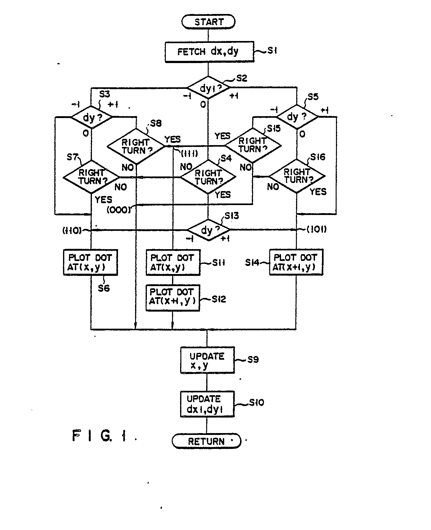
is performed such that a point (S6 in Fig. 1) on each line is written as one of two
end points thereof while a point (S14 in Fig. 1), offset by one point in the scan
direction, is written as the other of the two end points. The pattern data generating
system also includes a pattern data generating circuit (30) for, if w (w is a positive
integer) points b0, b1, ..., b(w-2), and b(w-1) are present on one scan line, writing
EXOR of data of points b0, b1, ..., b(j-1) at positions corresponding to points b(j)
(j is not less than 0 and less than w). Similar EXOR data writing is performed by
the pattern data generating circuit (30) for all the scan lines. Then, pattern data,
in which the area surrounded by the closed curve is filled or painted, is obtained.
|
|
