(19)
(11) EP 0 399 881 A3

(12) EUROPEAN PATENT APPLICATION

(88) Date of publication A3:
30.01.1991 Bulletin 1991/05

(43) Date of publication A2:
28.11.1990 Bulletin 1990/48

(21) Application number: 90401331.5

(22) Date of filing: 18.05.1990
(51) International Patent Classification (IPC)5H01L 29/41, H01L 21/82
(84) Designated Contracting States:
DE FR GB

(30) Priority: 20.05.1989 JP 127502/89

(71) Applicant: FUJITSU LIMITED
Kawasaki-shi, Kanagawa 211 (JP)

(72) Inventor:
  • Kajita, Tatsuya
    Tokyo 206 (JP)

(74) Representative: Joly, Jean-Jacques et al
Cabinet Beau de Loménie 158, rue de l'Université
F-75340 Paris Cédex 07
F-75340 Paris Cédex 07 (FR)


(56) References cited: : 


    (54) Semiconductor device having two conductor layers and production method thereof


    (57) A semiconductor device includes a base layer (1, 5), a chip region (CA) formed on the base layer, a peripheral region (PA) which surrounds the chip region on the base 
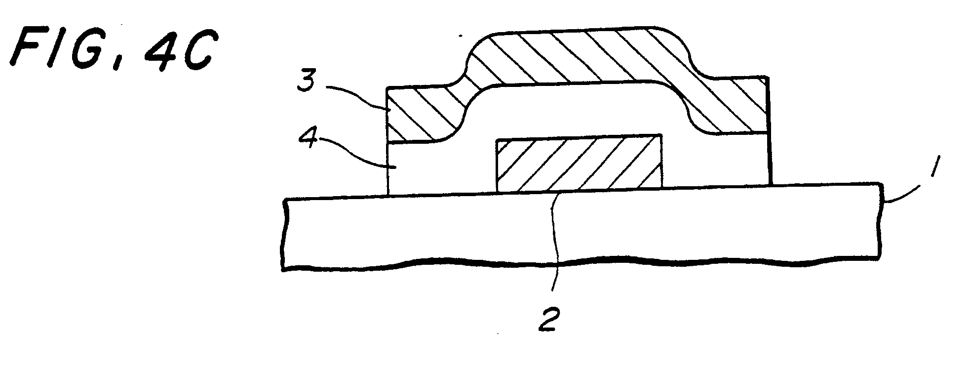
layer, and a patterned stacked structure formed on the base layer in both the chip region and the peripheral region, where the patterned stacked structure includes a lower layer (2) which is formed on the base layer, an intermediate layer (4) which is formed on the lower layer and an upper layer (3) formed on the intermediate layer. The upper layer and the intermediate layer are aligned to one side surface of the lower layer in at least a part of the chip region, and the intermediate layer and the upper layer cover one side surface of the lower layer in at least a part of the peripheral region.


    Search report