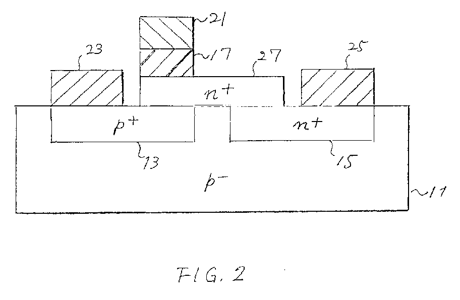
(57) A tunnel transistor comprises a semiconductor film (27) between a gate isolating
film (17) and parts of first (13) and second (15) semiconductor layers which are formed
in a substrate (11) to serve as source and drain regions with a spacer region left
therebetween and covered with the semiconductor film. The gate isolating film is over
the part of the first semiconductor layer and is made of either an insulating material
or a semiconductor material, each of which materials should have a wider forbidden
bandwith than a semiconductor material of the semiconductor film, such as silicon
dioxide, silicon nitride, or aluminium nitride, or gallium phosphide for silicon,
or AlGaAs for gallium arsenide. A source electrode is formed on an uncovered area
of the first semiconductor layer. The semiconductor film forms a tunnel junction with
the first semiconductor layer and an ohmic junction with the second semiconductor
layer, which junction may be either a homojunction or a heterojunction. The transistor
can be of a submicron order and is operable as either of depletion and enhancement
types of producing a great drain current at a high speed when supplied with no netavite
gate voltage and with a gate voltage.
|
|
