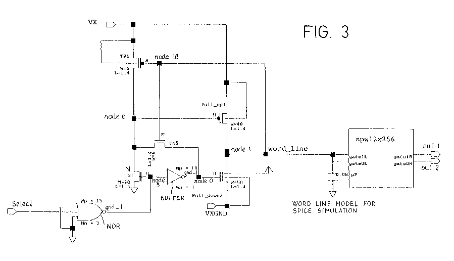
(57) A voltage translator circuit for driving the rows or wordlines of Flash EEPROM memories,
said translator circuit being arranged for receiving control logic voltages in the
range 0 to 3.3 volts, and operating voltages for performing reading, programming or
erasing operations in the range -9 to 12 volts, said translator circuit comprising
a decode section having a NOR gate circuit connected to an inverter circuit (BUFF)
through an input node (node 5) to couple a selection signal thereto, wherein:
- the wordline to be driven (node 1) is connected to ground (VXGND) through a first
N-MOS type switch transistor (pull-down 2) the gate of which (node 0) is driven by
a selection logic signal applied through said NOR gate and connected to the operation
voltage (VX) through a second P-MOS type switch transistor (pull-up 3),
- a first P-MOS type feedback transistor (TP4), having a gate (node 6) directly driven
by said wordline, said first feedback transistor being inserted between the operation
voltage (VX) and the gate region (node 6) of said second switch transistor (pull-up
3),
- a second N-MOS type feedback transistor (TN3), having a gate directly driven by said
wordline (node 18), said second feedback transistor being inserted between the connection
node (node 6) between said first feedback transistor (TP4) and the gate region of
said second switch transistor (pull-up 3) and the input node (node 0) on the gate
of said first switch transistor (pull-down 2).
|
|
