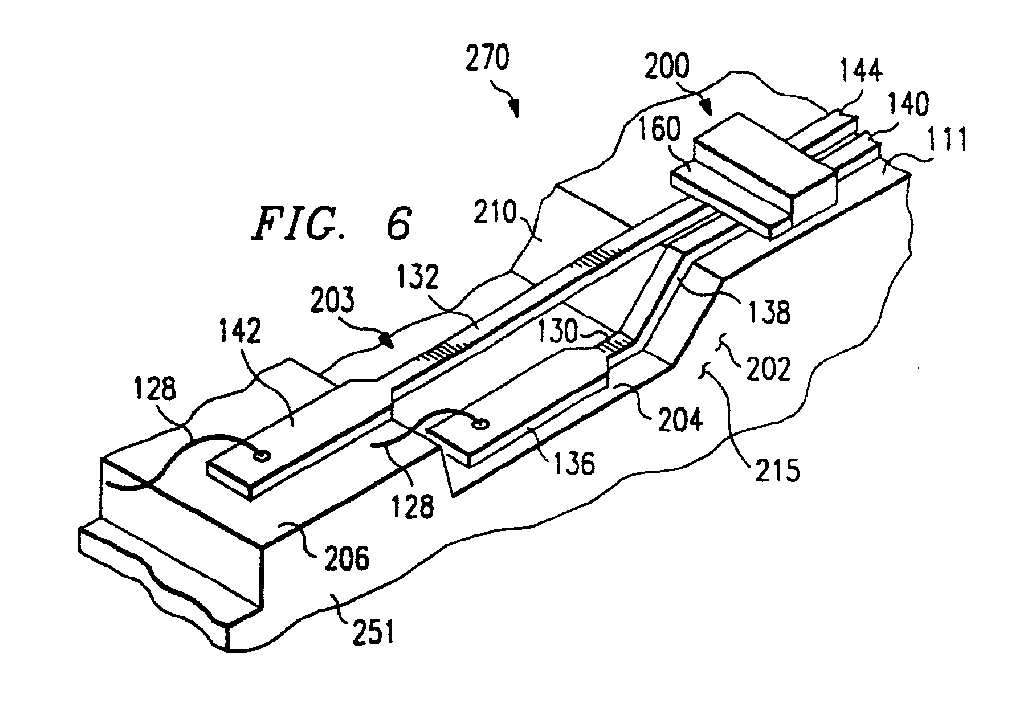
(57) A system (270, 370) for connecting a semiconductor chip (22, 322) to a leadframe
(12), the system (270, 370) includes a three-dimensional leadframe (12) and a bonding
support mechanism (202, 302, 402). The leadframe (12) may include a first lead (32,
132, 332, 432) having a first base portion (144), a first lead tip (42, 142, 342,
442), and a first longitudinal axis (305); a second lead (30, 130, 330, 430) having
a second base portion (140, 321), a second lead tip (36, 136, 336, 436), and a second
longitudinal axis. The first lead (32, 132, 332, 432) and second lead (30, 130, 330,
430) formed substantially adjacent to each other, and the second lead (30, 130, 330,
430) having a stepped portion (38, 138, 338, 438) such that the lead tips (42, 142,
342, 442, 36, 136, 336, 436) of the first lead (132, 332, 432) and second lead (130,
330, 430) are separated in a Z-direction (52) and in a Y-direction (52). The bonding
support mechanism (202, 302) for holding the three-dimensional leadframe (12) may
include a support body (215, 315), a trough (203, 303) formed on the support body
(215, 315). The trough (203, 303) may have a first surface (204, 304) at a first elevation,
where the first surface (204, 304) is for supporting the second lead tip (36, 136,
336). A second surface (206, 306) may be formed on the support body (215, 315) at
a second elevation and substantially adjacent to the first surface (204, 304). The
second surface (206, 306) is for supporting the first lead tip (42, 142, 342). The
first elevation and second elevation may be displaced from each other. The bonding
support mechanism (202, 302) may have an angled surface (210, 310) for accommodating
a stepped portion (38, 138, 338, 438) of the second lead (30, 130, 330) and may have
additional support surfaces (376, 319).
|
|
