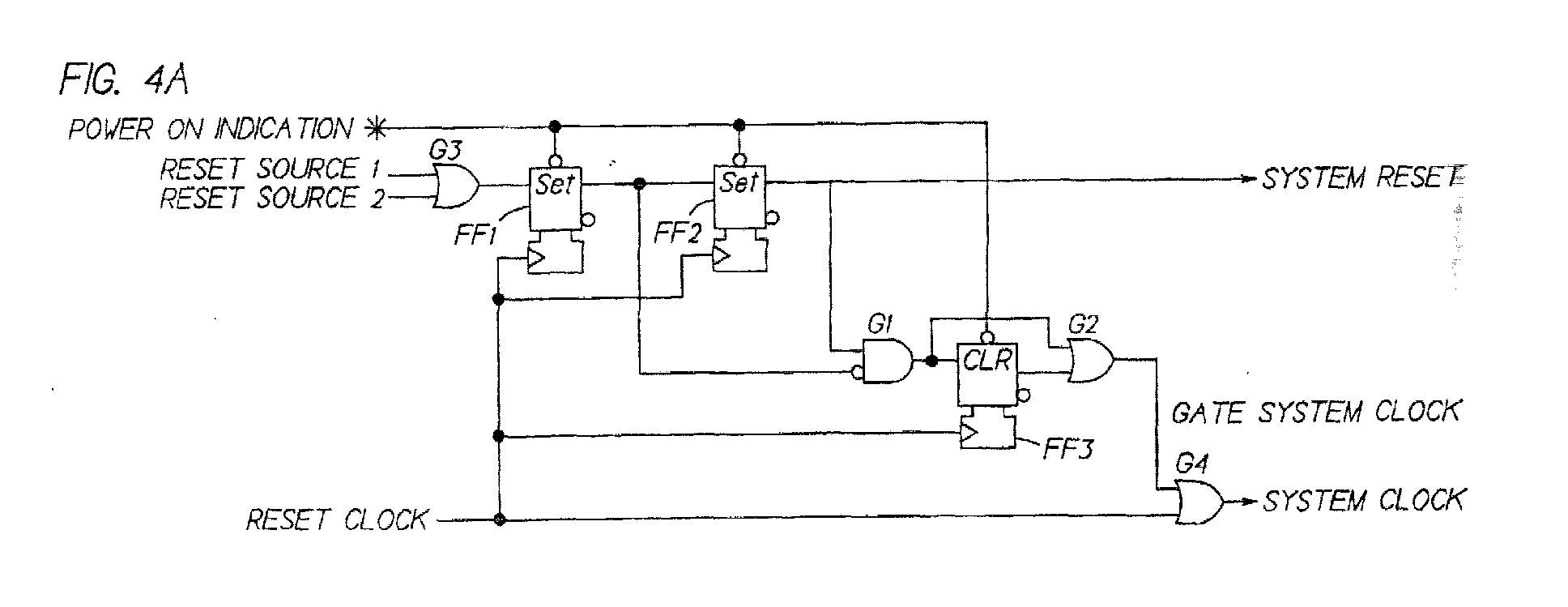
(57) Disclosed is a circuit and method for initializing clocked digital logic and for
generating a clock signal (system clock) for the clocked digital logic. The circuit
includes a flip-flop (FF1) that is responsive to a stimulus signal (reset source 1,2)
becoming active for asserting and then deasserting a reset signal (system reset) to
the clocked digital logic. The flip-flop (FF1) is clocked with a free-running clock
signal (reset clock). The circuit further includes a gating circuit (G4) for generating
the clock signal (system clock) from the free running clock signal (reset clock),
and an edge detector (G1,G2,FF3) that has an input coupled to the flip-flop (FF1)
and an output coupled to the gating circuit (G4). The edge detector (G1,G2,FF3) operates
to cause the gating circuit (G4) to place the clock signal (system clock) into an
inactive state at least one period of the free running clock (reset clock) prior to
the reset signal (system reset) being deasserted, and for holding the clock signal
(system clock) in the inactive state for at least one period of the free running clock
(reset clock) subsequent to the reset signal (system reset) being deasserted. In this
manner it is guaranteed that no clock edges are applied to the clocked digital logic
(e.g., flip-flops) for a predetermined period of time prior to and after the deassertion
of the reset signal (system reset). The period of the free running clock signal (reset
clock) is predetermined to exceed the minimum setup and hold times for the flip-flops
that comprise the clocked digital logic.
|
|
