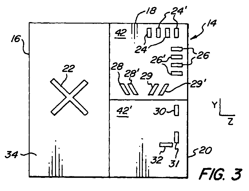
(57) A positioning, alignment, and image quality system comprising a detector (14) having
a photosensitive surface covered with an opaque layer having predetermined openings
(22,24,24',26,26',28,28',29,29',30-32) therein; a matched reticle (15) having predetermined
apertures therein is used to project the image of the apertures onto the openings.
A plurality of different detectors are thereby formed on a single monolithic substrate
for providing positioning, alignment, and image quality information. Different sub-detectors
(16,18,20) provide general positioning information, fine alignment or position information,
and image quality information, such as optimum focus and astigmatism. In one embodiment,
a pair of rectangular openings having a predetermined distance therebetween is used.
An illumination pattern is projected between the rectangular openings filling a portion
of the rectangular openings thereby providing a signal. The signals from the two openings
are balanced or made equal to obtain positioning information or alignment of the reticle
and the detector, and correspondingly a wafer stage attached to the detector. Different
opening configurations in the opaque mask covering the photosensitive layer are used
to provide different imaging information. The present invention permits alignment
information to be obtained in a non-scanning system, as well as in a system using
pulsed illumination sources. Additionally, a plurality of sub-detectors may easily
be fabricated onto a monolithic detector providing different functions. The simple
and easily modified structure permits it to be easily adapted to provide a variety
of different alignment, positioning, and image quality information that is desirable
in photolithographic techniques, particularly those used in semiconductor manufacturing.
Alignment in the range of 2.5 nanometers may be obtained.
|
|
