(57) There is provided a semiconductor device including a semiconductor substrate (2),
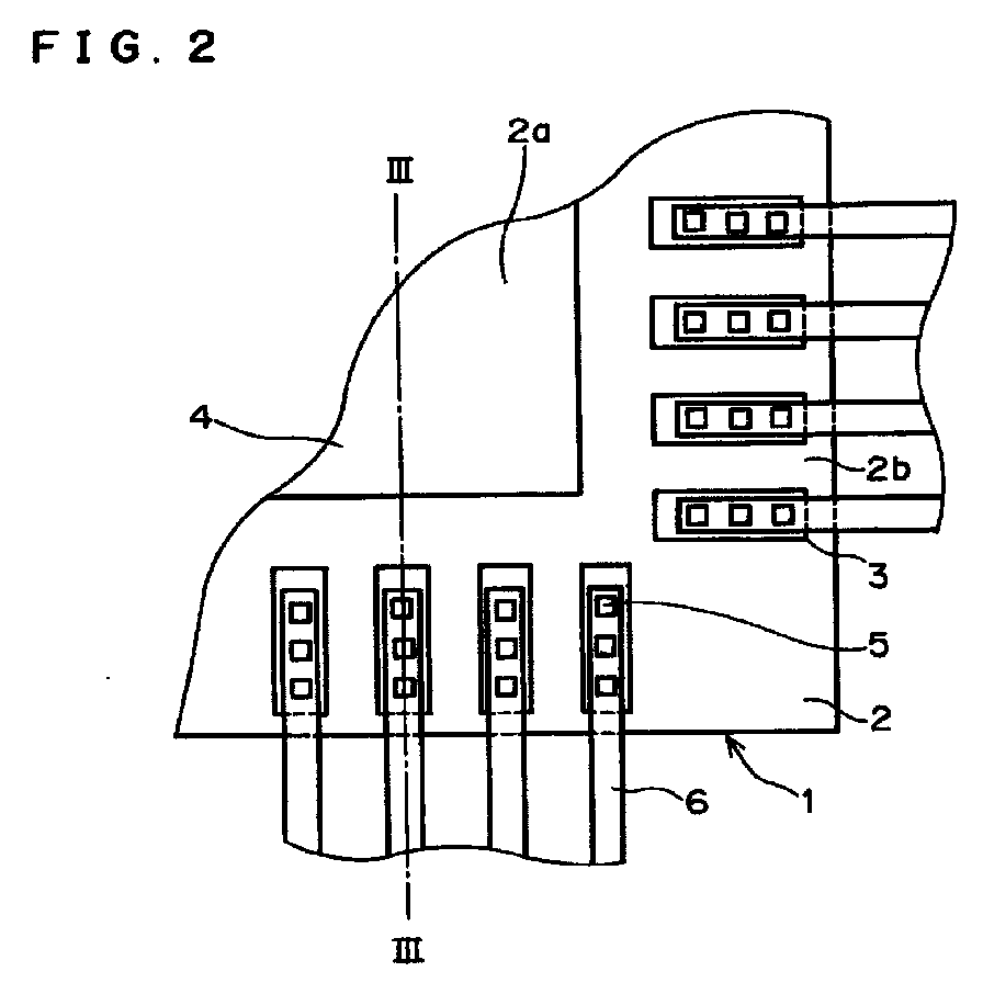
at least one electrode (3, 3a) formed on the semiconductor substrate (2), and an inner
lead (6) bonded to the electrode (3, 3a), characterized by that the inner lead (6)
is bonded to the electrode (3, 3a) at a plurality of bonding points (5, 5a). For instance,
the electrode (3) is shaped a rectangle having a longer side perpendicular to an edge
of the semiconductor substrate (2), and the bonding points (5) are arranged in a longitudinal
direction of the electrode (3). As an alternative, the electrode (3a) may be shaped
a square, in which case, the bonding points (5a) are arranged in a grid. The above-mentioned
semiconductor device provides a greater bonding area than a bonding area provided
by a single bonding point, which ensures greater bonding strength.
|
|
