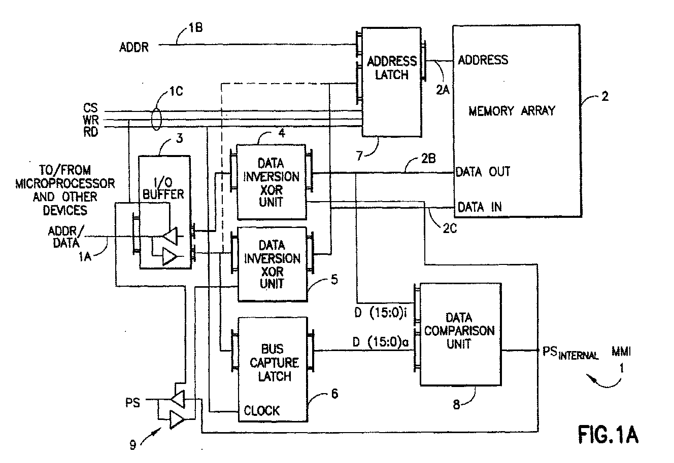
(57) A method for reducing the power consumption of an electronic system, such as a wireless
or cellular telephone, that has a memory 2 and a device for accessing the memory.
The method includes the steps of (a) during a first part of a memory access cycle,
applying an address over a bus 1A; (b) during a second part of the memory access cycle,
transferring data to or from the memory 2 over at least a portion of the bus 1A; and
(c) prior to the step of transferring, selectively inverting or not inverting the
data so as to minimize a number of bus signal lines 1C that are required to change
state between the first part and the second part of the memory access cycle. In a
preferred embodiment of the invention the bus 1A is a multiplexed address/data bus.
The method also generates a control signal PS that is transmitted to the bus 1A for
informing a receiving device that the data (or address) being transferred over the
multiplexed address/data bus 1A should be inverted before use. Also disclosed is a
memory 2 that operates in a burst mode by incrementing or decrementing memory addresses
using a clock signal, and that operates with the power saving circuitry to selectively
invert or not invert burst mode data read from or written to the memory.
|
|
