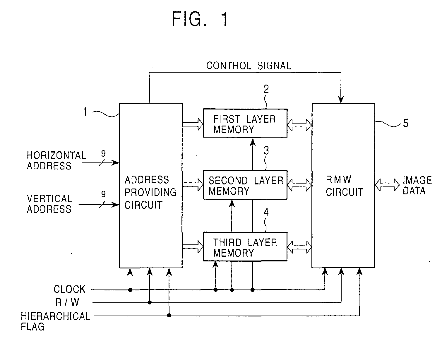
(57) Hierarchical coding may be performed without the need to employ a circuit for a line
delay, in addition to a memory for storing an image. An address providing circuit
(1) provides a 9-bit horizontal address and a 9-bit vertical address to a first layer
memory (2) while also providing, to a second layer memory (3), the eight higher order
bits of the horizontal address and the vertical address without the remaining least
significant bits. As a result, at the timing that each of the pixels in the first
layer is written on each of addresses (2s,2t), (2s+1,2t), (2s,2t+1) and (2s+1,2t+1)
in the first layer memory (2), the same address (s,t) in the second layer memory (3)
is accessed. Taking advantage of this, a read-modify-write circuit (5) determines
the sum of the storage values at the addresses (2s,2t), (2s+1,2t), (2s,2t+1), and
(2s+1,2t+1) in the first layer memory (2) and writes the sum on to the address (s,t)
in the second layer memory (3).
|
|
