(19)
(11) EP 0 905 536 A3

(12) EUROPEAN PATENT APPLICATION

(88) Date of publication A3:
13.11.2002 Bulletin 2002/46

(43) Date of publication A2:
31.03.1999 Bulletin 1999/13

(21) Application number: 98118137.3

(22) Date of filing: 24.09.1998
(51) International Patent Classification (IPC)7G02B 6/42, G02B 6/122, G02B 6/43
(84) Designated Contracting States:
AT BE CH CY DE DK ES FI FR GB GR IE IT LI LU MC NL PT SE
Designated Extension States:
AL LT LV MK RO SI

(30) Priority: 26.09.1997 JP 26118197
06.03.1998 JP 5499898

(71) Applicant: Nippon Telegraph and Telephone Corporation
Tokyo 163-8019 (JP)

(72) Inventors:
  • Hashimoto, Toshikazu Nippon Telegraph and Tel. Co.
    Tokyo 163-1419 (JP)
  • Yamada, Yasufumi Nippon Telegraph and Teleph. Co.
    Tokyo 163-1419 (JP)
  • Yanagisawa, Masahiro Nippon Telegraph and Tel. Co.
    Tokyo 163-1419 (JP)
  • Kato, Kuniharu Nippon Telegraph and Telephone. Co.
    Tokyo 163-1419 (JP)
  • Inoue, Yasuyuki Nippon Telegraph and Teleph. Co.
    Tokyo 163-1419 (JP)

(74) Representative: Pellmann, Hans-Bernd, Dipl.-Ing. et al
Patentanwaltsbüro Tiedtke-Bühling-Kinne & Partner Bavariaring 4-6
80336 München
80336 München (DE)


(54) Optical module


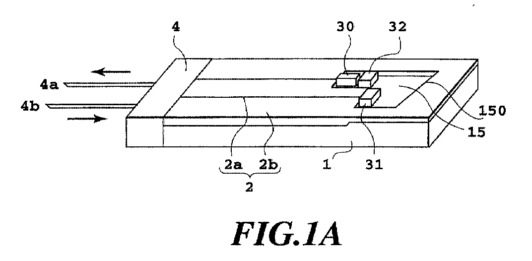
(57) In an optical module having a silicon substrate, a plurality of optical semiconductor devices (30, 31) and optical waveguides (2) for performing transmission of optical signals by the semiconductor devices integrated on the silicon substrate (1, 13), the silicon substrate is doped with an impurity to increase the number of carriers in the silicon substrate for suppressing optical crosstalk between the plurality of optical semiconductor devices, the optical waveguide (2) is composed of a core part (2a) and a peripheral cladding layer (2b) of the core part, or optical fibers each coupled with each of the semiconductor devices, and an electrical resistivity of part or all of the silicon substrate is 0.1Ωcm or less, or a lower part (7) of an optical semiconductor light receiving device is made high in resistance, and a lower part (6) of an optical semiconductor light emitting device is made low in resistance, in which construction, each of the optical semiconductor devices is locally coated with a transparent resin (9), and all the parts protruding upward from the optical waveguide are coated with a light absorbent such as one or plural caps (8, 81).


Search report