(19)
(11) EP 0 978 934 A3

(12) EUROPEAN PATENT APPLICATION

(88) Date of publication A3:
13.08.2003 Bulletin 2003/33

(43) Date of publication A2:
09.02.2000 Bulletin 2000/06

(21) Application number: 99113780.3

(22) Date of filing: 14.07.1999
(51) International Patent Classification (IPC)7H02M 7/48, H02M 7/00
(84) Designated Contracting States:
AT BE CH CY DE DK ES FI FR GB GR IE IT LI LU MC NL PT SE
Designated Extension States:
AL LT LV MK RO SI

(30) Priority: 04.08.1998 JP 22030498

(71) Applicant: KABUSHIKI KAISHA TOSHIBA
Kawasaki-shi, Kanagawa-ken 210-8572 (JP)

(72) Inventors:
  • Kijima, Kenji
    1-1 Shibaura 1-chome Minato-ku Tokyo 105 (JP)
  • Omura, Ichiro
    1-1 Shibaura 1-chome Minato-ku Tokyo 105 (JP)
  • Saito, Suzuo
    1-1 Shibaura 1-chome Minato-ku Tokyo 105 (JP)

(74) Representative: Henkel, Feiler, Hänzel 
Möhlstrasse 37
81675 München
81675 München (DE)


(54) Power conversion system


(57) [Object] To obtain a power conversion system that is capable of achieving low inductance, improving cooling performance and making the external shape of the entire system small.
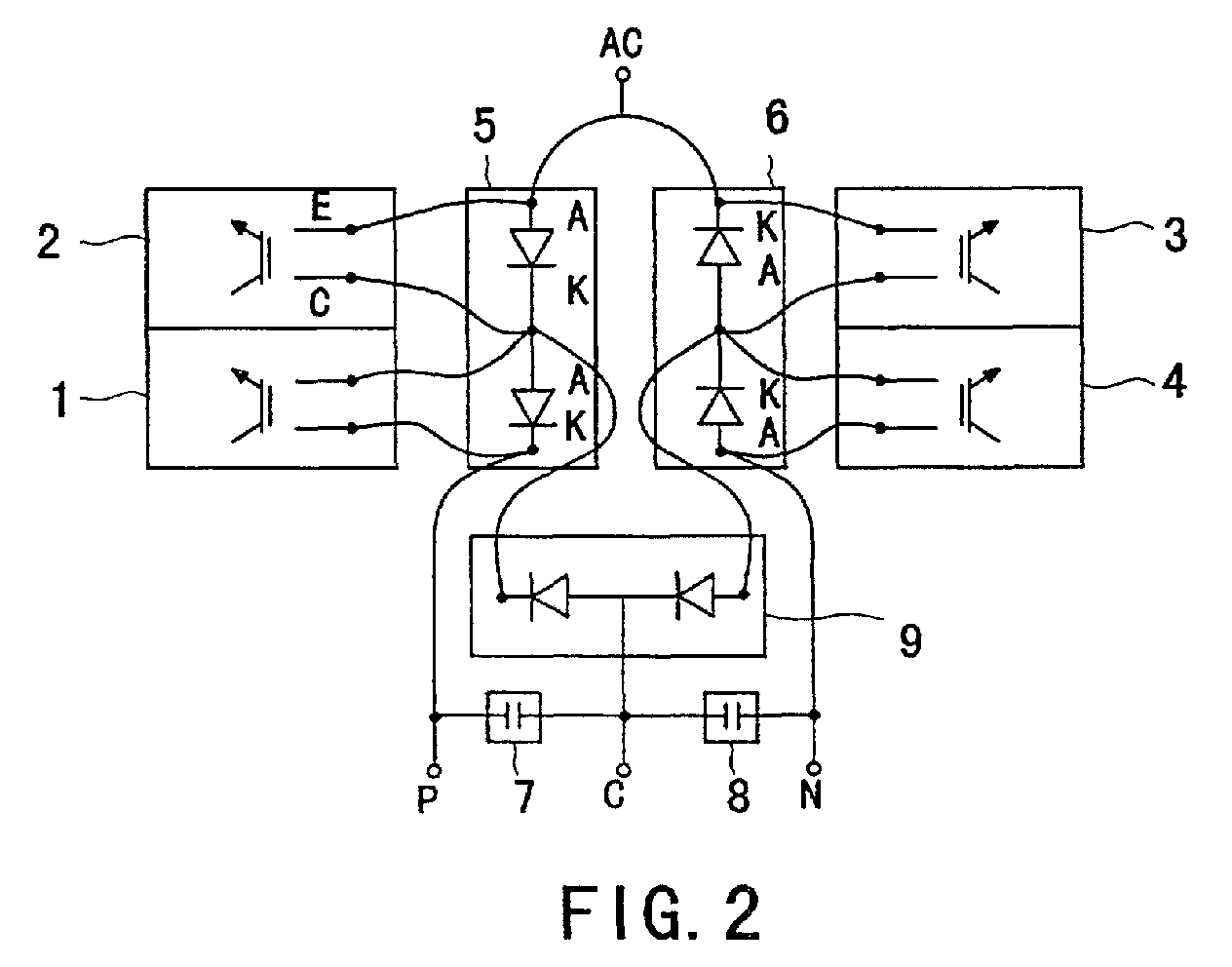
[Construction] A power conversion system comprising a combination of a plurality of single phase inverter units, wherein the inverter units are composed of first ∼ fourth device packages each of which is composed of packaged power devices 1∼4, two pieces of neutral point clamp diodes 9, first and second by-pass diode packages which are composed of packaged first, second, third and fourth by-pass diodes 5, 6, clamp diode packages which are composed of packaged clamp diodes, and the first and second by-pass diode packages are provided on one of the wall surfaces of the clamp diode package and the first, second and third, fourth device packages are provided on the outside wall surfaces of the by-pass diode package, respectively.


Search report