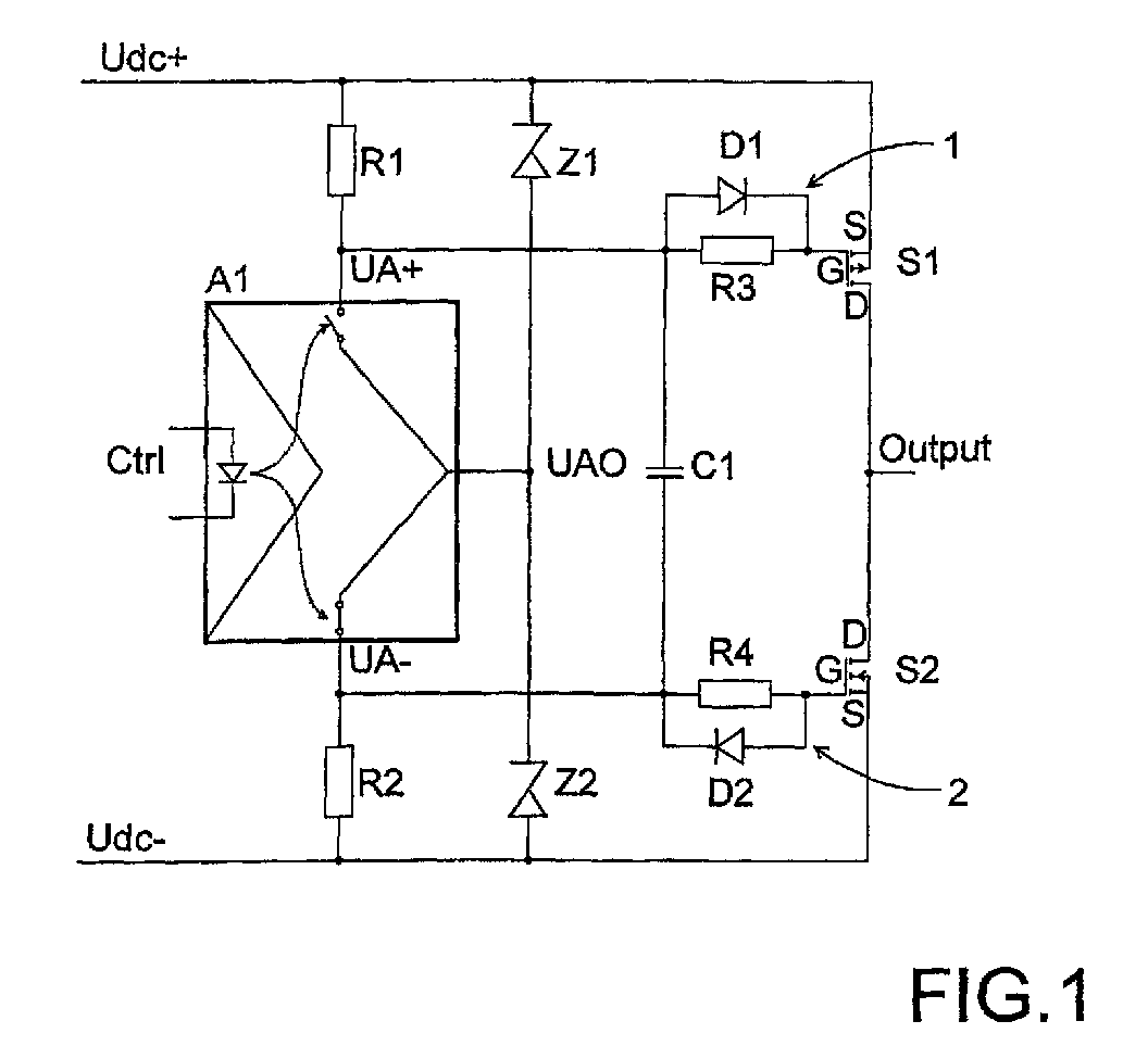
(57) A control circuit for controlling a power semiconductor, the control circuit comprising
a gate driver (A1) comprising a control input (Ctrl), auxiliary voltage inputs (UA+,
UA-) and an output (UAO). The control circuit further comprises a first semiconductor
switch (S1) comprising a control electrode (G) and main electrodes (S, D), a first
main electrode (S) forming a positive input pole (Udc+) of the control circuit and
a second (D) forming an output (Output) of the control circuit; a second semiconductor
switch (S2) comprising a control electrode (G) and main electrodes (S, D), a first
main electrode (S) forming a negative input pole (Udc-) of the control circuit and
a second (D) being connected to the output (Output) of the control circuit; a first
resistance (R1), a second resistance (R2), a first zener diode (Z1) whose anode is
connected to the output (UAO) of the gate driver (A1) and whose cathode to the positive
input pole (Udc+) of the control circuit; and a second zener diode (Z2) whose cathode
is connected to the output (UAO) of the gate driver (A1) and whose anode to the negative
input pole (Udc-) of the control circuit.
|
|
