(19)
(11) EP 1 022 605 A3

(12) EUROPEAN PATENT APPLICATION

(88) Date of publication A3:
16.08.2000 Bulletin 2000/33

(43) Date of publication A2:
26.07.2000 Bulletin 2000/30

(21) Application number: 00108030.8

(22) Date of filing: 01.03.1991
(51) International Patent Classification (IPC)7G02F 1/035
(84) Designated Contracting States:
AT BE CH DE DK ES FR GB GR IT LI LU NL SE

(30) Priority: 02.03.1990 JP 5202290

(62) Application number of the earlier application in accordance with Art. 76 EPC:
95108382.3 / 0677765
91301729.9 / 0444959

(71) Applicant: FUJITSU LIMITED
Kawasaki-shi, Kanagawa 211-8588 (JP)

(72) Inventors:
  • Seino, Minoru
    Atsugi-shi, Kanagawa 243 (JP)
  • Mekada, Naoyuki
    Hadano-shi, Kanagawa 257 (JP)
  • Doi, Masaharu
    Atsugi-shi, Kanagawa 243 (JP)
  • Nakazawa, Tadao
    Hiratsuka-shi, Kanagawa 254 (JP)
  • Kubota, Yoshinobu
    Ayase-shi, Kanagawa 252 (JP)

(74) Representative: Fenlon, Christine Lesley et al
Haseltine Lake & Co., Imperial House, 15-19 Kingsway
London WC2B 6UD
London WC2B 6UD (GB)


(54) Optical waveguide device


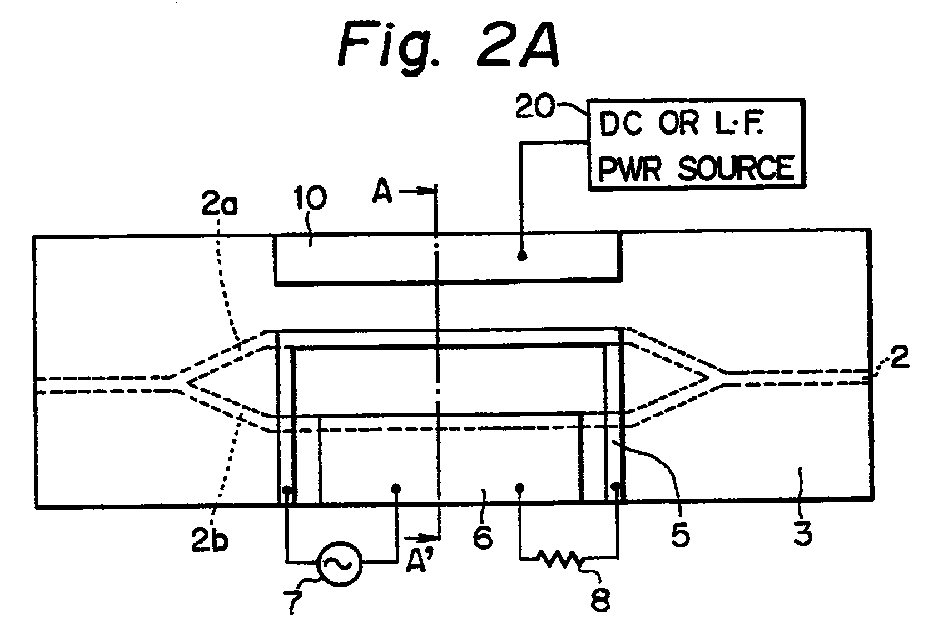
(57) An optical waveguide device comprising an optical waveguide (2, 2a, 2b) formed on a surface of a substrate (1) having an electro-optical effect, a pair of electrodes (5, 6) formed on a corresponding region above the optical waveguide (2, 2a, 2b) and receiving a driving electric signal thereacross, and a buffer layer (3) formed all over the substrate (1) including the optical waveguide (2, 2a, 2b), has a third electrode (10, 10a) formed on a corresponding region above the substrate (1), wherein a distribution of an electric field occurring in a vicinity of the optical waveguide (2, 2a, 2b) by an application of the electric signal is greatly changed in accordance with a change in a frequency of the electric signal, the third electrode (10, 10a) comprising a semiconductive layer and being disposed on the region spaced with a predetermined distance from the pair of electrodes (5, 6) formed on the corresponding regions above the optical waveguide (2, 2a, 2b) and being coupled to a direct current voltage, a low frequency voltage or a ground.


Search report