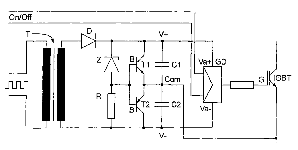
(57) A stabilized gate driver which comprises a current source transformer (T) which comprises
a primary and a secondary coil, and a gate driver unit (GD) which comprises a positive
auxiliary voltage input (Va+) and a negative auxiliary voltage input (Va-). The gate
driver also comprises a diode (D) the anode of which is connected to the positive
pole of the secondary coil of the current source transformer (T), a zener diode (Z)
the cathode of which is connected to the cathode of the diode (D), resistance (R)
whose one pole is connected to the anode of the zener diode (Z) and the other pole
to the negative pole of the secondary coil of the current source transformer (T),
a first semiconductor switch (T1) the control electrode (B) of which is connected
to the point between the zener diode and the resistance, and the collector of which
is connected to the cathode of the zener diode, a second semiconductor switch (T2)
the control electrode (B) of which is connected to the point between the zener diode
and the resistance and the collector of which is connected to the negative pole of
the secondary coil of the current source transformer (T) and the emitter to the emitter
of the first semiconductor switch (T1), a first capacitance (C1) the first pole of
which is connected to the collector of the first semiconductor switch (T1) and the
second pole to the emitter of the second semiconductor switch (T1), the first pole
of the capacitance (C1) forming a positive voltage input (V+) which is connected to
the positive auxiliary voltage input (Va+) of the gate driver unit (GD), and a second
capacitance (C2) the first pole of which is connected to the emitter of the second
semiconductor switch (T2) and the second pole to the collector of the second semiconductor
switch (T2), the second pole of the capacitance (C2) forming a negative voltage input
(V-) which is connected to the negative auxiliary voltage input (Va-) of the gate
driver unit (GD), in which case the point between the capacitances (C1, C2) forms
the zero potential (Corn) between the positive (V+) and the negative (V-) auxiliary
voltage input.
|
|
