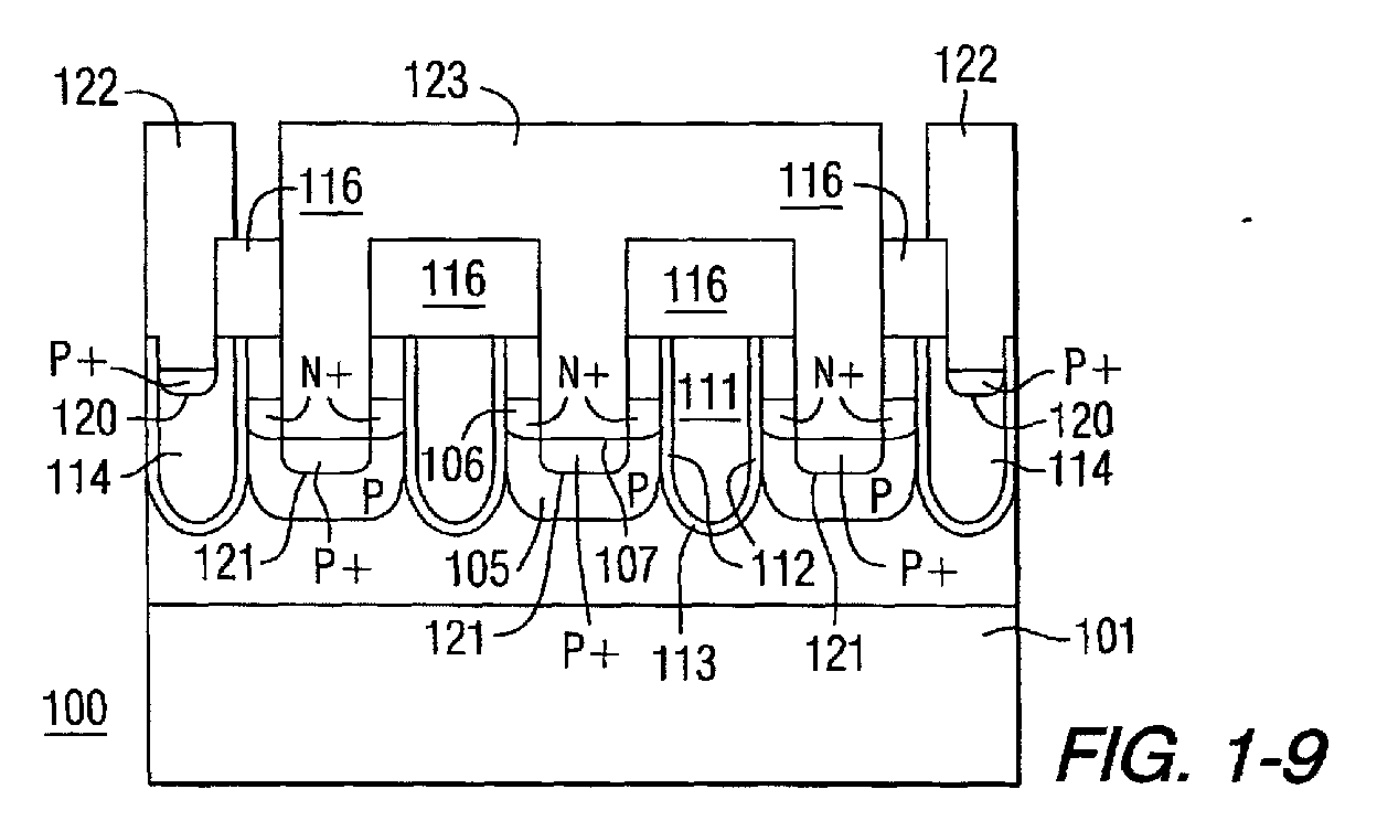
(57) A process for forming an MOS-gated device having sell-aligned trenches, a screen
oxide layer is formed on an upper layer of a semiconductor substrate, and a nitride
layer is formed on the screen oxide layer. Using a well mask, the nitride layer is
patterned and etched to define a well region in the upper layer, and ions of a first
conduction type are diffused into the masked upper layer to form the well region.
Ions of a second, opposite conduction type are implanted into the well region of the
masked upper layer to form a source region extending to a selected depth that defines
a source-well junction. The well mask is removed, exposing the portion of the nitride
layer previously underlying the mask. An oxide insulating layer providing a hard mask
is formed overlying the well and source regions in the upper layer. The remaining
portions of the nitride layer and the screen oxide layer underlying it, which had
been protected by the well mask, are removed, exposing the portion of the substrate
not masked by the oxide insulating layer.
The portion of the substrate thus exposed is etched to form a gate trench extending
through the substrate to a selected depth beneath the well region. Sidewalls and a
floor of an insulator are formed in the gate trench, which is filled with a semiconductor.
The semiconductor in the trench is planarized to be substantially coplanar with the
upper surface of the oxide insulating layer. An interlevel dielectric layer is formed
on the planarized gate trench semiconductor and the upper surface of the oxide insulating
layer.
|
|
