(57) Useful, new electronic devices are disclosed which utilize the huge polarization
and electric double layer generated by excimer formation reaction in solid thin host
films doped with excimer forming atoms (rare-gases and halogens: hereinafter, the
parent atoms of excimers) at ambient temperature and pressure. A fundamental type
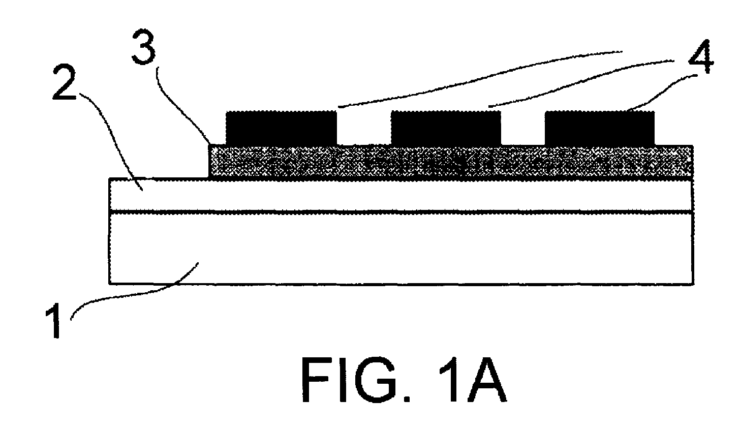
of these devices is a single layer solid-state excimer device, which consists of a
thin film (3) fabricated by selecting a material from insulating metal oxides, at
least one dopant from the parent rare-gas atoms (Ar, Kr and Xe) of excimers, and at
least one dopant from parent halogen atoms (F, Cl, Br and I) of excimers. The dopants
can be doped in the thin film during its fabrication process. Upper and lower electrodes
(4,2) can be added to the thin film when they are needed, and practical devices can
be obtained by fabricating the electrodes and thin film together on a substrate (1),
which can be useful in ferroeletric memory applications.
|
|
