(57) A nonvolatile memory that has a plurality of floating gate type cell transistors
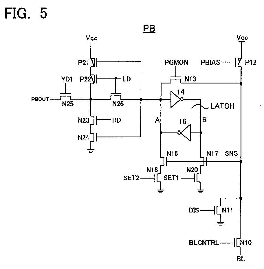
(MC0,MC1,...) comprises a read buffer circuit (PB), connected to the bit line, that
detects the threshold voltage states in the cell transistor. Each cell transistor
can hold 2N threshold voltage states and accordingly, the read buffer circuit reads N bits of
data. For this purpose, the read buffer circuit has a latch circuit (LATCH) that latches
the read data in accordance with the detected threshold voltage state. This latch
circuit has a first (N17, N20) and second (N16, N18) latch reversal circuit for reversing
the latched state to the first or second state. When the read buffer circuit (PB)
reads the first bit being held in the cell transistor, the latch circuit in its initial
state is reversed or not reversed by the first latch reversal circuit (N17, N20) in
accordance with the detected first and second threshold voltage state, or third and
fourth threshold voltage state, and that latch state is output as the first data.
Furthermore, when the lower order second bit held in the cell transistor is read next,
the read buffer circuit is reversed or not reversed from the latch state corresponding
to the first data above by the first latch reversal circuit in accordance with the
detected first or second threshold voltage state. Then, it is reversed or not reversed
by the second latch reversal circuit (N16, N18) in accordance with the detected third
or fourth threshold voltage state and the latch state is output as the second data.
|
|
