(57) An optimal write conductor layout structure for improved MRAM performance is disclosed.
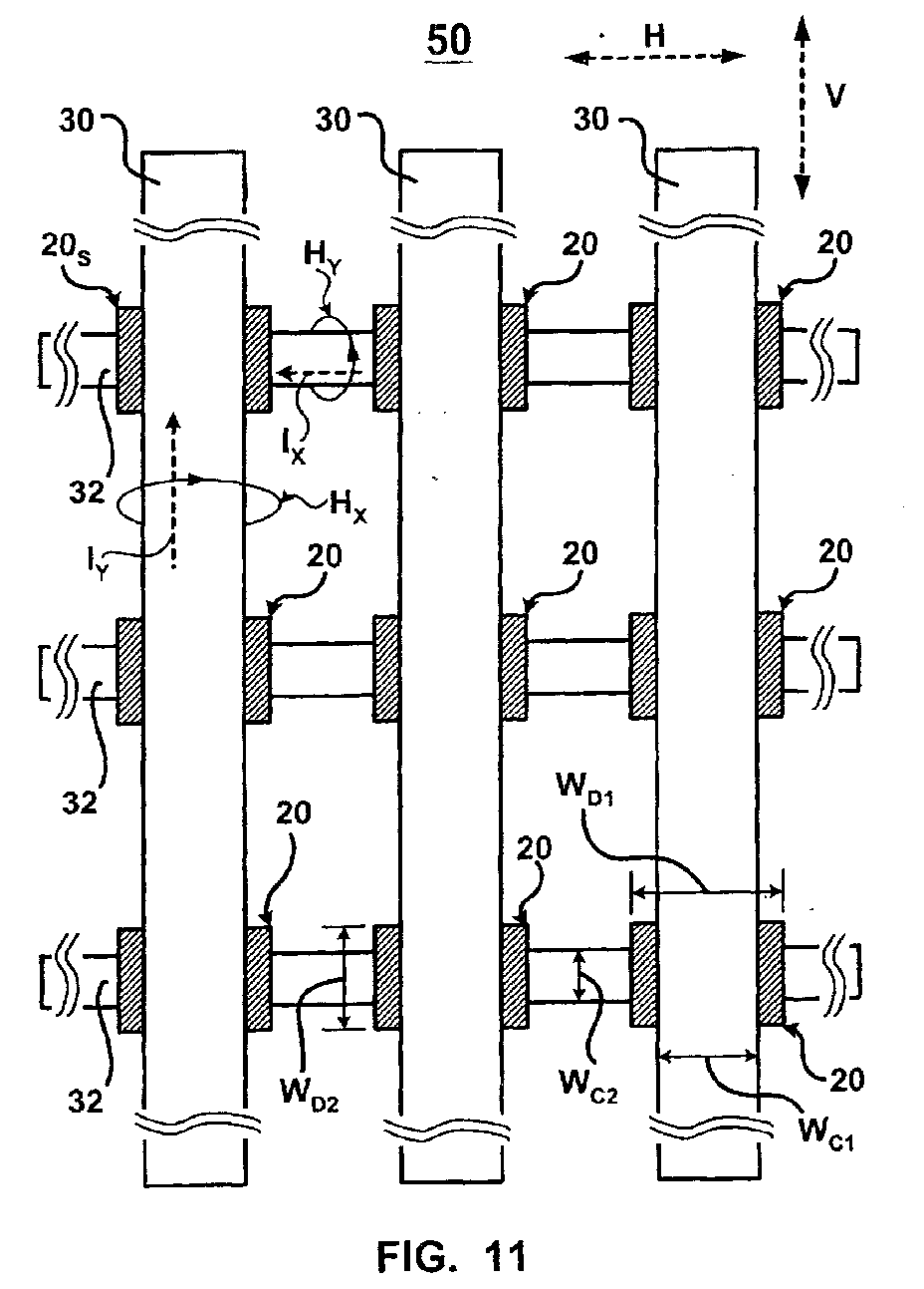
A write conductor layout structure (10) for a magnetic memory cell includes a data
storage layer (20) having a first layer width (WD1) in a first direction (V) and a second layer width (WD2) in a second direction (H). The data storage layer (20) is positioned between a first
conductor (30) having a first width (WC1) in the first direction (V) and a second conductor (320 having a second width (WC2) in the second direction (H). The first and second conductors (30, 32) cross the
data storage layer (20) in the first and second direction (V, H) respectively. The
first width (WC1) of the first conductor (30) is less than the first layer width (WD1) of the data storage layer (20) and the first width (WC1) of the first conductor (30) is positioned so that the first layer width (WD1) overlaps the entirety of the first width (WC1) of the first conductor (30). The second width (WC2) of the second conductor (32) is less than the second layer width (WD2) of the data storage layer (20) and the second width (WC2) of the second conductor (32) is positioned so that the second layer width (WD2) overlaps the entirety of the second width (WC2) of the second conductor (32). The narrow widths of the first and second conductors
(30, 32) eliminates misalignment between the conductors (30, 32) and the data storage
layer (20), reduces leakage of a write magnetic field (HX, HY) generated by currents (IY, IX) applied to the first and second conductors (30, 32), and can generate the write
magnetic field (HX, HY) with less current thereby reducing power consumption in the memory cell.
|
|
