(57) The invention regards a content addressable memory, which, for example, may be implemented
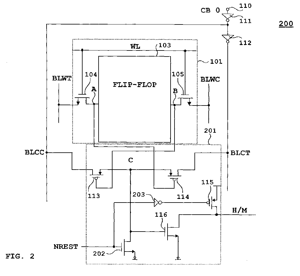
in a data processing system or a data processor and comprises at least a first single
bit storage (101; 301), a word line (WL), at least one bit write line (BLWT, BLWC)
and a hit/miss line (H/M), and at least a first single bit compare circuit (201; 320),
said first single bit storage comprises at least a first output (A; A0) and said first
single bit compare circuit comprises at least a first compare bit input (BLCT; CB
0) and two field effect transistors (113, 114; 312, 313).
Particularly, in order to reduce the power consumption, said first output (A; A0)
of said single bit storage (101; 301) is applied to the gate of only one, a first
field effect transistor (114; 312) of said two field effect transistors (113, 114;
312, 313). For an additional reduction of the power consumption two single bit storages
(101, 301) are connected to a shared compare circuit (319). In case of a mismatch,
only one out of four compare nodes (C0, C1, C2, C3) of the shared compare circuit
is switched high, i.e. changes its potential.
|
|
