(19)
(11) EP 1 207 598 A3

(12) EUROPEAN PATENT APPLICATION

(88) Date of publication A3:
23.10.2002 Bulletin 2002/43

(43) Date of publication A2:
22.05.2002 Bulletin 2002/21

(21) Application number: 01126412.4

(22) Date of filing: 07.11.2001
(51) International Patent Classification (IPC)7H01S 5/183
(84) Designated Contracting States:
AT BE CH CY DE DK ES FI FR GB GR IE IT LI LU MC NL PT SE TR
Designated Extension States:
AL LT LV MK RO SI

(30) Priority: 20.11.2000 JP 2000353113

(71) Applicant: Kabushiki Kaisha Toshiba
Tokyo 105-8001 (JP)

(72) Inventor:
  • Tanaka, Akira
    Yokohama-shi, Kanagawa-ken (JP)

(74) Representative: HOFFMANN - EITLE 
Patent- und Rechtsanwälte Arabellastrasse 4
81925 München
81925 München (DE)


(54) Surface emitting semiconductor laser


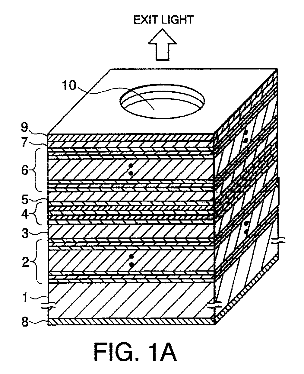
(57) A surface emitting semiconductor laser capable of improving high temperature properties is provided. In a surface emitting semiconductor laser, a well width of an active layer (4) is set at from 4 nm to 6 nm and the number of wells thereof is set at one or two. In addition, above and below the active layer (4), InGaAlP system clad layers (3,5) are formed, and in a stacking direction of the active layer (4), through the above and below clad layers (3,5) each, further above and below thereof, light reflecting layers (2,6) are formed.


Search report