(19)
(11) EP 1 215 669 A3

(12) EUROPEAN PATENT APPLICATION

(88) Date of publication A3:
12.01.2005 Bulletin 2005/02

(43) Date of publication A2:
19.06.2002 Bulletin 2002/25

(21) Application number: 01310557.2

(22) Date of filing: 18.12.2001
(51) International Patent Classification (IPC)7G11B 7/24, G11B 7/0045, G11B 7/26
(84) Designated Contracting States:
AT BE CH CY DE DK ES FI FR GB GR IE IT LI LU MC NL PT SE TR
Designated Extension States:
AL LT LV MK RO SI

(30) Priority: 18.12.2000 JP 2000383346

(71) Applicant: MATSUSHITA ELECTRIC INDUSTRIAL CO., LTD.
Kadoma-shi, Osaka 571-8501 (JP)

(72) Inventors:
  • Kitaura, Hideki
    Souraku-gun, Kyoto 619-0237 (JP)
  • Yamada, Noboru
    Hirakata-shi, Osaka 573-1104 (JP)

(74) Representative: Jeffrey, Philip Michael 
Frank B. Dehn & Co. 179 Queen Victoria Street
London EC4V 4EL
London EC4V 4EL (GB)


(54) Optical information recording medium, method for producing the same, and method and apparatus for recording information theron


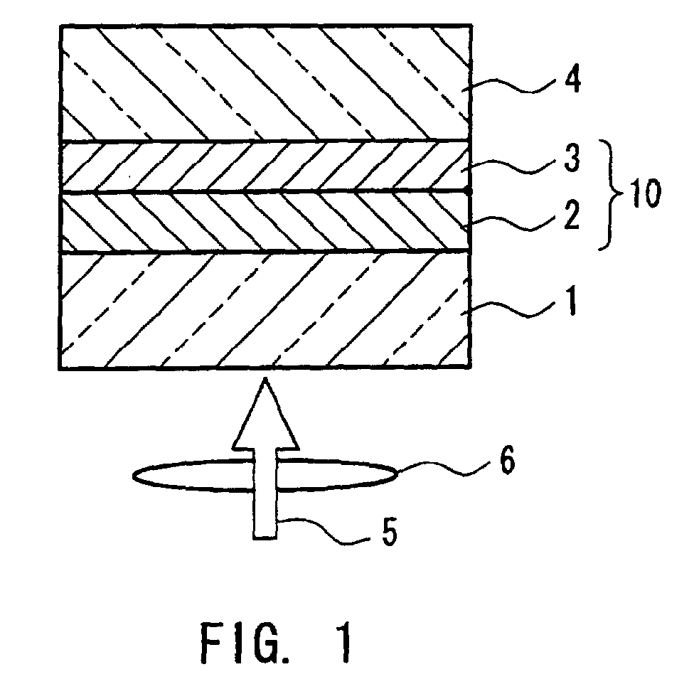
(57) The present invention provides a write-once optical information recording medium that can achieve a high reflectance and favorable recording and reproducing characteristics such that a high C/N ratio and high sensitivity even when information is recorded/reproduced with high density. This medium includes a transparent substrate (1) and at least one information layer (2) formed on the substrate. The information layer includes a recording layer made of a material including Te, O and M, where M is at least one element selected from the group consisting of Al, Si, Ti, V, Cr, Mn, Fe, Co, Ni, Cu, Zn, Ga, Ge, Zr, Nb, Mo, Ru, Rh, Pd, Ag, In, Sn, Sb, Hf, Ta, W, Re, Os, Ir, Pt, Au and Bi. A reflectance with respect to a light beam incident from the side of the transparent substrate after recording information on the recording layer is lower than a reflectance before recording.


Search report