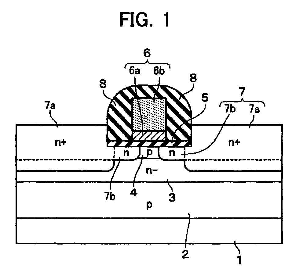
(57) A semiconductor device includes a semiconductor substrate, a gate electrode as formed
over a surface of the substrate with a gate dielectric film interposed therebetween,
source/drain layers formed in said semiconductor substrate to oppose each other with
a channel region residing between these layers at a location beneath the gate electrode,
the source/drain layers each having a low resistivity region and an extension region
being formed to extend from this low resistivity region toward the channel region
side and being lower in impurity concentration and shallower in depth than the low
resistivity region, a first impurity-doped layer of a first conductivity type formed
in the channel region between the source/drain layers, a second impurity-doped layer
of a second conductivity type formed under the first impurity-doped layer, and a third
impurity-doped layer of the first conductivity type formed under the second impurity-doped
layer, wherein the first impurity-doped layer is equal or less in junction depth than
the extension regions of the source/drain layers whereas the second impurity-doped
layer is designed in impurity concentration and thickness to be fully depleted due
to a built-in potential as created between the first and third impurity-doped layers.
|
|
