(19)
(11) EP 1 235 250 A3

(12) EUROPEAN PATENT APPLICATION

(88) Date of publication A3:
07.04.2004 Bulletin 2004/15

(43) Date of publication A2:
28.08.2002 Bulletin 2002/35

(21) Application number: 01401744.6

(22) Date of filing: 29.06.2001
(51) International Patent Classification (IPC)7H01J 29/28
(84) Designated Contracting States:
AT BE CH CY DE DK ES FI FR GB GR IE IT LI LU MC NL PT SE TR
Designated Extension States:
AL LT LV MK RO SI

(30) Priority: 26.02.2001 JP 2001050877
26.02.2001 JP 2001050879

(71) Applicant: SONY CORPORATION
Tokyo (JP)

(72) Inventors:
  • Jun, Miura, c/o Sony Fukushima Corporation
    Adachi-gun, Fukushima-ken (JP)
  • Koichi, Furui
    Shinagawa-ku, Tokyo (JP)

(74) Representative: Thévenet, Jean-Bruno et al
Cabinet Beau de Loménie 158, rue de l'Université
75340 Paris Cédex 07
75340 Paris Cédex 07 (FR)


(54) Transfer foil, transfer method, transfer apparatus, flat cathode-ray tube, and its manufacturing method


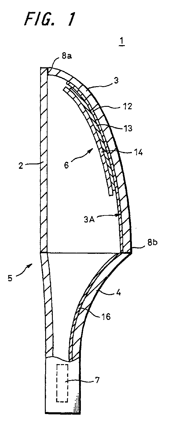
(57) A reflection type flat cathode-ray tube (1) enhanced in quality of display image, and its manufacturing method are presented. A flat cathode-ray tube (1) is composed by forming a grid layer (12), a reflective layer (13), and a fluorescent layer (14) sequentially at the inner side (3A) of a screen panel (3). The reflective layer (13) is preferably formed at the inner side of the circumference of the fluorescent layer (14). On a transfer substrate, a transfer foil laminating at least a fluorescent layer (14), a reflective layer (13), and a grid layer (12) in this order is prepared, the grid layer side of the transfer foil is heated, pressed and adhered to the inner side of a screen panel (3), a transfer substrate is peeled off, and a fluorescent screen composed of the fluorescent layer (14), reflective layer (13), and grid layer (12) is transferred.


Search report