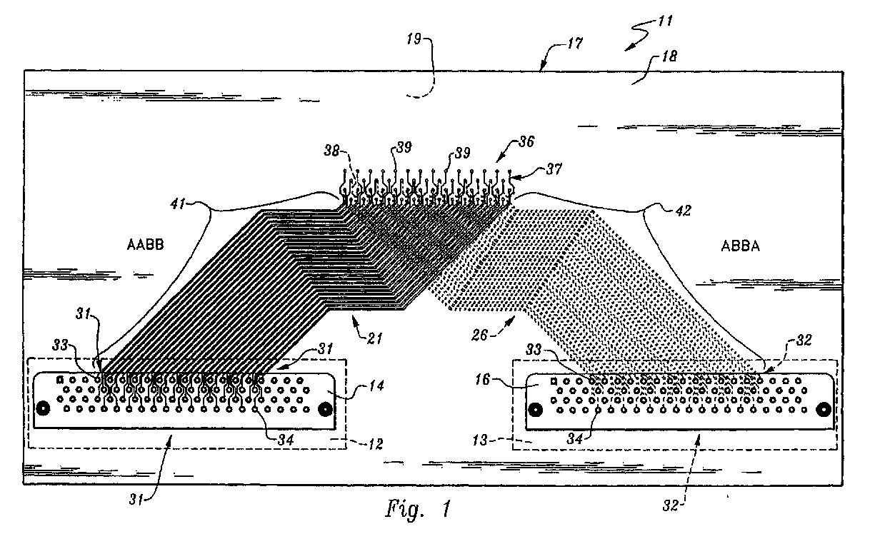
(57) A circuit board (17) including differential bus traces (21, 26, 106, 107) on or buried
within both sides of the board, interconnecting electronic devices (12, 13) such as
disk drives, processors, and connectors for external cables. Via trace fields (36,
), which mimic the size and configuration of the device and cable connector fields
(31, 32), are located between each connector (14, 16) on the board. The via fields
link bus traces (21, 106) on or within one side of the board with respective bus traces
(26, 107) on or within the other side of the board. The via fields (37, 38) may include
subtle, unequal undulations in the trace patterns to provide equalization in the lengths
of all trace pairs. The via fields (37, 38) and the connector fields (31, 32) both
include repetitive conductor order reversals in the trace connections on opposing
sides of the board, to reduce crosstalk between channels. The via fields (36, 73)
may be oriented parallel with respect to collinearly arranged devices (12, 13), or
orthogonal with respect to devices or connectors which are parallel (71, 72). Where
a connector has laterally offset groups of pin connections (79, 81, 82), a via field
may also include offset groups of vias (83, 84, 86) to provide trace length equalization.
|
|
