|
(11) | EP 1 255 386 B1 |

| (12) | EUROPEAN PATENT SPECIFICATION |
|
|
| (54) |
Line equaliser for compensation of droop effect Leitungsentzerrer zur Kompensation von Droop-Effekten Egalisateur de ligne de compensation des effets de droop |
|
|
||||||||||||||||||||||||||||
| Note: Within nine months from the publication of the mention of the grant of the European patent, any person may give notice to the European Patent Office of opposition to the European patent granted. Notice of opposition shall be filed in a written reasoned statement. It shall not be deemed to have been filed until the opposition fee has been paid. (Art. 99(1) European Patent Convention). |
BACKGROUND OF THE INVENTION
[0002] Integrated Circuits (IC) generally need to be tested to assure proper operation. This - in particular - is required during IC development and manufacturing. In the latter case, the ICs are usually tested before final application. During test, the IC, as device under test (DUT), is exposed to various types of stimulus signals, and its responses are measured, processed and usually compared to an expected response of a good device. Automated test equipments (ATE) usually perform these tasks according to a device-specific test program. Examples for ATE are the Agilent 83000 and 93000 families of Semiconductor Test Systems of Agilent Technologies. Details of those families are also disclosed e.g. in EP-A-859318, EP-A-864977, EP-A-886214, EP-A-882991, EP-A-1092983, US-A-5,499,248, US-A-5,453,995.
[0003] Signals generally experience some degradation due to more or less lossy transmission paths, usually referred to as 'Droop Effect'. In particular when reaching higher frequencies beyond several hundred MHz, such signal degradation becomes more and more important and has to be considered in design and applications.
[0004] In digital test and measurement applications, e.g. ATE applications, it has to be made sure that the rise time at the output of a transmission path stimulated by a voltage step at the input is sufficiently lower than the rise time of pulses to be measured. Otherwise, pulse rise times cannot be measured accurately.
[0005] Sawai A., et. al. describes in "COAXIAL PCM TRANSMISSION USING DUOBINARY SCHEME" NEC Research and Development, Nippon Electric Ltd. Tokyo, April 1981, pages 89-96, an approach for accurate waveform equalization for a high speed transmission. An equalization scheme is described using three kinds of circuits, namely fixed equalizers for amplitude and phase equalization, flat gain amplifiers and a
AGC circuit.
[0006] EP 0 467 412 A2 describes a digital adaptive equalizer which equalizes received signals through digital filtering operations by changing filtering coefficients. It comprises a coefficient calculating unit for calculating the filtering coefficients through functionally transforming one kind of parameters, such as distance, by using it as an input to a function corresponding to the respective ones of said filtering coefficients and a filtering operation executing unit for executing digital filtering operations based on the respective one of the filtering coefficients. A variable lag filter for adjusting the phase delay of received signals is provided. A coefficient converting unit calculates a part or all of tap coefficients of the filter by converting at least one piece of timing control information.
[0007] US-A-4,768,205 describes a switched capacitor adaptive line equalizer for use in a digital communication system which is adapted to receive input signals at a plurality of signal rates and to supply equalized output signals. Input signals are sent through a switched capacitor equalizer which includes a low-pass filter in order to control the frequency band of the input signals and a variable gain action which selectively sets a prescribed characteristic in response to the output of the low-pass filter. A control circuit responsive to the output of the switched capacitor equalizer and the input signal rate selectively adjusts to the characteristic of the switched capacitor equalizer means. Input signals are processed on a time division basis in two channels of the variable gain section, to select the operating characteristic on one of the channels while another operation is performed on the other channel.
SUMMARY OF THE INVENTION
[0008] It is an object of the invention to improve higher frequency measurement applications. The object is achieved by a filter of claim 1. Preferred embodiments are defined in the dependent claims.
[0009] According to the present invention, a filter is applied between a digital signal source and a signal receiver for providing compensation for droop caused in a transmission path between the signal source and the signal receiver.
[0010] The filter is designed to provide a high pass characteristics substantially approximating or following in a relevant frequency range an attenuation function substantially proportional to
or - when denoting attenuation in dB - substantially proportional to the square root of the frequency. Thus, droop effects dominated by skin effect in the relevant frequency range can be efficiently compensated, wherein the filter comprises a plurality of different filter stages each substantially following an attenuation characteristic characterized by asymptotic behaviors for higher and for lower frequencies and a transition behavior between the two asymptotic behaviors. The difference between the attenuation values of the asymptotes for higher and for lower (e.g. DC-attenuation) frequencies represents a measure for the attenuation of each stage and shall be referred to as the 'stage attenuation'. It is clear, however, that this stage attenuation need not necessarily represent the maximum possible attenuation of the stage. In particular overswing behaviors, e.g. towards the asymptotes, might cause higher attenuation values than the stage attenuation.
[0011] A center frequency can be assigned to each transition behavior representing a frequency in the center of the transition behavior. The center frequency can be determined e.g. by a reversal or turning point in the transition, a mean frequency of the transition behavior range, or as the point in frequency where the stage has half of its stage attenuation. However, it is to be understood that the center frequency only represents a tool for characterizing the attenuation behavior over frequency of each stage, but is not to be interpreted in a sense e.g. of providing precisely the 'center' of the transition behavior range.
[0012] The plurality of filter stages is preferably designed such that the transition behaviors are distributed over the relevant frequency range. Preferably, the center frequencies of the stages are distributed over the relevant frequency range. In one embodiment, the relevant frequency range is divided into a plurality of sub-ranges and each sub-range will be dominated by the transition behavior of one stage. It is clear that a certain overlapping of the transition behaviors of different stages might occur, in particular dependent on the number and width of the sub-ranges. A higher overlapping will generally occur with increasing number of stages/sub-ranges.
[0013] The plurality of filter stages is further preferably designed such that the stage attenuation increases with increasing center frequency.
[0014] The attenuation characteristics of the different filter stages superimpose to the attenuation characteristics of the (entire) filter.
[0015] While it is clear that approximation of the square root behavior can be improved with increasing number of stages, it has to be considered that also parasitic effects generally increase with increasing number of stages. In a preferred embodiment, 3 stages are provided already allowing to sufficiently approximating the square root behavior.
[0016] In a preferred embodiment, the filter comprises a plurality of stages each having the same schematics or arrangement of components but with different component values. Thus, the characteristics off all stages are the same in principle, and the individual characteristic can be adjusted by selecting the component values. This significantly fosters designing of the filter. Preferably, the stages are arranged in series, however parallel or even mixed arrangements can also be applied.
[0017] Preferably, each stage comprises two resistors (preferably with substantially same resistance value) in series, with a third resistor being coupled between the two. A capacitor is coupled parallel to the two resistors, and an inductor is connected in series with the third resistor (preferably between the third resistor and ground). This T- or star-arrangement of resistors represents a standard attenuator circuit known in the art. Such attenuator circuit, when designed for an environment of characteristic impedance Z and terminated at its output with impedance Z, will attenuate signals from its input to output by a defined, frequency-independent amount and will not reflect any portion of the signal present at its input. Other equivalent topologies for the attenuator are commonly referred to as "Pi" and "Bridged T".
[0018] Preferably, the capacitor and inductor values are chosen (matched?) such that L = Z2C. This will ensure that the capacitor and the inductor contribute to the transition behavior of the stage at the same frequency and that, over the entire frequency range, the whole stage will not reflect any portion of the signal present at its input.
[0019] The values of the resistors determine the DC-attenuation (i.e. the asymptote for lower frequencies), while the matched values of capacitor and inductor determine the transition and thus the center frequency of each stage. Such stages are preferably arranged in series.
[0020] In another preferred embodiment, the stages of the filter are designed in a combined arrangement. Preferably, the filter comprises two resistors (preferably with substantially same resistance value) in series with a third resistor coupled between the two. An inductor is connected in series with the third resistor thus representing a first stage. A first capacitor in series with a resistor is coupled in parallel to the two resistors thus representing a second stage. A second capacitor with or without a resistor in series is further coupled in parallel to the two resistors thus representing a third stage. This T- or star-arrangement of resistors represents the same standard attenuator circuit as explained above. . The values of the resistors each determine the DC-attenuation (i.e. the asymptote for lower frequencies), while the values of the capacitors and the inductor each determine the transition and thus the center frequency of each stage. Contrary to the above-illustrated embodiment, it is therefore not possible to match each capacitor to an inductor (and vice versa) such that reflections are minimized.
[0021] In one embodiment, the principle characteristic of the filter can be designed in two different ways: Firstly, since the filter will result in an attenuation of the signal to be compensated, the filter attenuation will be determined by the maximum acceptable attenuation for the signals. Since the filter substantially approximates a square root behavior of the attenuation over the frequency, this maximum acceptable attenuation for the signals translates into a maximum applicable frequency of the filter. Secondly and opposite to the first way, a given maximum applicable frequency of the filter will translate accordingly to a maximum attenuation of the filter. In case the filter attenuation exceeds the maximum acceptable attenuation for the signals, signal amplification stages might be provided.
[0022] The invention can be partly or entirely supported by one or more suitable software programs, which can be stored on or otherwise provided by any kind of data carrier, and which might be executed in or by any suitable data processing unit. Software programs or routines are preferably applied for designing the filter and its stages.
[0023] The inventive filter is preferably applied in an ATE as signal recovery before receiving the response signals to be measured and processed (e.g. by comparing to an expected response of a good device). Thus signal rise times degraded by the transmission path between the DUT and the receiving unit of the ATE can be efficiently recovered allowing to measure the DUT with significantly improved accuracy.
BRIEF DESCRIPTION OF THE DRAWINGS
[0024] Other objects and many of the attendant advantages of the present invention will be readily appreciated and become better understood by reference to the following detailed description when considering in connection with the accompanied drawings. Features that are substantially or functionally equal or similar will be referred to with the same reference sign(s).
- Fig. 1
- illustrates the principle application of a filter 10 according to the present invention.
- Figs. 2
- show simulated attenuation characteristics of a model transmission path 30 and of a 'ideal' high pass characteristic of the filter 10.
- Figs. 3 and 4
- illustrate examples for designing the filter 10.
DETAILED DESCRIPTION OF THE INVENTION
[0025] In Fig. 1, a signal response 20 of a DUT in an ATE (as introduced in the introductory part of the description) is degraded in a transmission path 30 resulting in a degraded signal response 40. The filter 10 provides signal compensation to the degraded signal response 40 resulting in a compensated signal response 50 eventually received by the ATE and further processed.
[0026] Due to the attenuation of both the transmission path 30 and the filter 10, it is clear that the resulting signal level of the compensated signal response 50 can be significantly decreased with respect to the signal level of the signal response 20. Signal amplification might be required.
[0027] In the preferred ATE application of the filter 10, the clock rate for the provision of the DUT stimulus signals is in the range of 200MHz to 2GHz.
[0028] Fig. 2A shows a simulated attenuation characteristic based on a model of the transmission path 30 dominated by skin effect for frequencies in the range of 1MHz and 100GHz, and more preferably between 50MHz to 20GHz. Following the applied model here, the simulated attenuation characteristic is proportional to the square root of the frequency. Accordingly for fully compensating all signal degradation caused by the transmission path 30, the filter 10 has to be designed to provide a high pass characteristic inversely approximating or following the attenuation function of Fig. 2A. Such 'ideal' high pass characteristic of the filter 10 substantially proportional to the square root of the frequency is illustrated in Fig. 2B.
[0029] Figs. 3 illustrates a first example for designing the filter 10. Fig. 3A shows the circuit of the filter 10 with three filter stages 300A, 300B, and 300C. Each stage 300 comprises two resistors (with same resistance values) in series with a third resistor coupled between the two. A capacitor is coupled parallel to the two resistors, and an inductor is connected in series with the third resistor. This T-arrangement of resistors avoids reflections. The values of the resistors determine the DC-attenuation of each stage, while the values of capacitor and inductor together determine the transition and thus the center frequency of each stage. Such stages are preferably arranges in series.
[0030] Figs. 3B-3D illustrate the attenuation characteristic of each stage 300, and Fig. 3E shows the attenuation characteristic of the entire filter 10 as the superimposed characteristics of all three stage 300A, 300B, and 300C. In all Figs. 3B-3E, the x-axis goes from 10MHz to 100GHz, while the y-axis goes from 0dB to +10dB attenuation. Fig. 3B corresponds to stage 300A, Fig. 3C corresponds to stage 300B, and Fig. 3D corresponds to stage 300C.
[0031] Stage 300A (with the two resistors of 10.89Ω, the third resistor of 109.34Ω, the capacitor of 2pF, and the inductor of 5nH) shows an asymptote for lower frequencies (usually referred to as DC-attenuation) of 3.85dB, an asymptote for higher frequencies of 0dB, a transition therebetween from about 1GHz to 10GHz, and a center frequency (where the stage has about half of its maximum attenuation) of about 3.6GHz.
[0032] Stage 300B (with the two resistors of 4.42Ω, the third resistor of 280.91Ω, the capacitor of 20pF, and the inductor of 100nH) shows an asymptote for lower frequencies of 1.54dB, an asymptote for higher frequencies of 0dB, a transition therebetween from about 100MHz to 1GHz, and a center frequency of about 450MHz.
[0033] Stage 300C (with the two resistors of 1.77Ω, the third resistor of 705.58Ω, the capacitor of 800pF, and the inductor of 2µH) shows an asymptote for lower frequencies of 0.61 dB, an asymptote for higher frequencies of 0dB, a transition therebetween from about 20MHz to 200MHz, and a center frequency of about 57MHz.
[0034] The superimposition of all three stages 300A, 300B, and 300C in Fig. 3E shows an asymptote for lower frequencies of 3.85 + 1.54 + 0.61 = 6.00dB, an asymptote for higher frequencies of 0dB. The superimposition already comes close to the 'ideal' high pass characteristic of Fig. 2B being substantially proportional to the square root of the frequency.
[0035] Each of the three stages 300A, 300B, and 300C shows, over the entire frequency range, substantially no reflection with infinitely accurate component values and less than -80dB for the values given in Fig. 3A. The same applies for the superimposition of all three stages in Fig. 3E.
[0036] Figs. 4 illustrate a second preferred example of a design for the filter 10. Fig. 4A shows the circuit of the filter 10 with three filter stages 400A, 400B, and 400C. Comparing the circuit of Figs. 4A and 3A immediately makes clear that the term 'stage' is not limited to a serial design as in Fig. 3A, but also covers combined serial and parallel connections of functional stage units.
[0037] The filter 10 - again - comprises two resistors (here: each 16.6Ω) in series with a third resistor (here: 67Ω) coupled between the two. An inductor (here: 3.3nH) is connected in series with the third resistor thus representing the first stage 400A. A first capacitor (here: 5.6pF) is coupled in parallel to the two resistors thus representing the second stage 400B. A second capacitor (here: 12pF) with a resistor (here: 80Ω) in series is further coupled in parallel to the two resistors thus representing the third stage 400C. This T-arrangement of resistors also avoids reflections.
[0038] Fig. 4B shows a simulation of the filter 10 according to Fig. 4A with the attenuation characteristic 410 and the reflection characteristic 420. The filter shows an asymptote for lower frequencies of about 6dB and an asymptote for higher frequencies of 0dB. The superimposition - again - comes close to the 'ideal' high pass characteristic of Fig. 2B.
[0039] Each of the capacitors and the inductor in Fig. 4A are determined by the desired center frequency of their corresponding stage. It is therefore not possible to match each capacitor to an inductor (and vice versa) such that reflections are minimized. The maximum of the reflection characteristic 420 in the example of Fig. 4B is thus at just - 16dB.
[0040] Fig. 4C shows actual spectral measurements. Reference sign 430 depicts the attenuation characteristic of the transmission path 30 showing the droop effect for higher frequencies. Reference sign 440 depicts the attenuation characteristic of the filter 10 according to Fig. 4A, and reference sign 450 shows the combined attenuation characteristic of both the transmission path 30 and the filter 10 according to Fig. 4A. In contrast to attenuation characteristic 430 of the transmission path 30, the combined attenuation characteristic 450 shows an 'almost flat' attenuation characteristic until about 5GHz. However, due to the attenuation of both the transmission path 30 and the filter 10, the resulting signal level of the compensated signal response 50 will be significantly decreased.
[0041] Figs. 4D and 4E illustrate the effect of the filter 10. While both Figs. 4D and 4E depict actual measurements using the embodiment of Fig. 4A for the filter 10, similar results could be shown e.g. for the filter 10 according to Fig. 3A. Fig. 4D shows the measured response signal 40 (without filter 10) for a 625 Mbit/s clock signal, and the compensated response signal 50 as the signal 40 after being applied to the filter 10 and after being level-compensated.
[0042] Fig. 4E illustrates the effect of the filter 10 in a so-called eye-diagram for a 3.6Gbit/s PRBS-signal as signal 20 (refer to Fig. 1). While the eye-diagram for the compensated response signal 50 is almost open - indicating a significantly improved Bit-Error-Rate behavior, much shorter rise-times and fall-times, more clearly defined high and low levels and a significantly reduced amount of data-dependent jitter -the eye-diagram for the measured response signal 40 (without filter 10) is significantly closed causing higher Bit-Error-Rates values.
1. A filter (10) adapted to be applied between a digital signal source (20) and a signal
receiver for providing compensation for droop caused in a transmission path (30) between
the signal source (20) and the signal receiver, the filter comprising a high pass
characteristic substantially approximating or following in a relevant frequency range
an attenuation function substantially proportional to
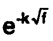
or - when denoting attenuation in dB - substantially proportional to the square root of the frequency
characterized in that
the filter (10) comprises a plurality of different filter stages (300A, 300B, 300C; 400A, 400B, 400C) each substantially following an attenuation characteristic characterized by asymptotic behaviors for higher and for lower frequencies and a transition behavior between the two asymptotic behaviors, the attenuation characteristics of the different filter stages (300A, 300B, 300C; 400A, 400B. 400C) superimposing to attain the attenuation characteristics of the filter (10).
or - when denoting attenuation in dB - substantially proportional to the square root of the frequency
characterized in that
the filter (10) comprises a plurality of different filter stages (300A, 300B, 300C; 400A, 400B, 400C) each substantially following an attenuation characteristic characterized by asymptotic behaviors for higher and for lower frequencies and a transition behavior between the two asymptotic behaviors, the attenuation characteristics of the different filter stages (300A, 300B, 300C; 400A, 400B. 400C) superimposing to attain the attenuation characteristics of the filter (10).
2. The filter of claim 1, wherein the plurality of filter stages (300A, 300B, 300C; 400A,
400B, 400C) is designed such that the transition behaviors are distributed over the
relevant frequency range.
3. The filter of claim 2, wherein the center frequencies of the stages (300A, 300B, 300C;
400A, 400B, 400C) are distributed over the relevant frequency range.
4. The filter of one of claims 1 to 3, wherein relevant frequency range is divided into
a plurality of sub-ranges and each sub-range will be dominated by the transition behavior
of one stage (300A, 300B, 300C; 400A, 400B, 400C).
5. The filter of one of claims 1 to 4, wherein the plurality of filter stages (300A,
300B, 300C; 400A, 400B, 400C) is designed such that the stage attenuation increases
with increasing center frequency.
6. The filter of one of claims 1 to 5, wherein the filter (10) comprises three filter
stages (300A, 300B, 300C; 400A, 400B, 400C).
7. The filter of one of claims 1 to 6, wherein the filter (10) comprises a plurality
of stages (300A, 300B, 300C; 400A, 400B, 400C) each having the same arrangement of
components or schematics but with different component values.
8. The filter of claim 7, wherein each stage (300A, 300B, 300C) comprises two resistors
in series with a third resistor coupled between the two resistors, a capacitor being
coupled parallel to the two resistors, and an inductor being connected in series with
the third resistor, preferably between the third resistor and ground.
9. The filter of one of claims 1 to 5, wherein the filter (10) comprises two resistors
in series, a third resistor coupled between the two resistors, an inductor being connected
in series with the third resistor, a first capacitor in series with a resistor being
coupled in parallel to the two resistors, and a second capacitor with or without a
resistor in series being coupled in parallel to the two resistors.
10. The filter of one of claims 1 to 9, wherein the relevant frequency range is in the
range of 1 MHz to 100GHz, and preferably in the range of 50MHz to 20GHz.
11. A measuring device adapted to receive a response signal (20), the response signal
(20) being degraded by a transmission path (30), comprising a filter (10) of one of
claims 1 to 10 for compensating the degraded response signal (40).
12. An automated test equipment adapted for providing a stimulus signal to a device under
test - DUT - and to receive a response signal (20) representing the response of the
DUT to the stimulus signal, wherein the response signal (20) is degraded by a transmission
path (30), the automated test equipment comprising a filter (10) of one of claims
1 to 10 for compensating the degraded response signal (40).
1. Ein Filter (10), das angepasst ist, um zwischen einer Digitalsignalquelle (20) und
einem Signalempfänger angewendet zu werden, zum Bereitstellen einer Kompensation eines
Absinkens, das in einem Übertragungspfad (30) zwischen der Signalquelle (20) und dem
Signalempfänger bewirkt wird, wobei das Filter eine Hochpasscharakteristik aufweist,
die in einem relevanten Frequenzbereich im Wesentlichen einer Dämpfungsfunktion nahe
kommt oder folgt, die im Wesentlichen proportional zu
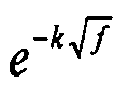
oder - wenn eine Dämpfung in dB angemerkt wird - im Wesentlichen proportional zu der Quadratwurzel der Frequenz ist,
dadurch gekennzeichnet, dass
das Filter (10) eine Mehrzahl unterschiedlicher Filterstufen (300A, 300B, 300C; 400A, 400B, 400C) aufweist, die alle im Wesentlichen einer Dämpfungscharakteristik folgen, die durch asymptotisches Verhalten für höhere und für niedrigere Frequenzen und ein Übergangsverhalten zwischen den beiden asymptotischen Verhaltensweisen gekennzeichnet ist, wobei sich die Dämpfungscharakteristika der unterschiedlichen Filterstufen (300A, 300B, 300C; 400A, 400B, 400C) überlagern, um die Dämpfungscharakteristika des Filters (10) zu erzielen.
oder - wenn eine Dämpfung in dB angemerkt wird - im Wesentlichen proportional zu der Quadratwurzel der Frequenz ist,
dadurch gekennzeichnet, dass
das Filter (10) eine Mehrzahl unterschiedlicher Filterstufen (300A, 300B, 300C; 400A, 400B, 400C) aufweist, die alle im Wesentlichen einer Dämpfungscharakteristik folgen, die durch asymptotisches Verhalten für höhere und für niedrigere Frequenzen und ein Übergangsverhalten zwischen den beiden asymptotischen Verhaltensweisen gekennzeichnet ist, wobei sich die Dämpfungscharakteristika der unterschiedlichen Filterstufen (300A, 300B, 300C; 400A, 400B, 400C) überlagern, um die Dämpfungscharakteristika des Filters (10) zu erzielen.
2. Das Filter gemäß Anspruch 1, bei dem die Mehrzahl von Filterstufen (300A, 300B, 300C;
400A, 400B, 400C) derart entworfen ist, dass die Übergangsverhaltensweisen über den
relevanten Frequenzbereich verteilt sind.
3. Das Filter gemäß Anspruch 2, bei dem die Mittenfrequenzen der Stufen (300A, 300B,
300C; 400A, 400B, 400C) über den relevanten Frequenzbereich verteilt sind.
4. Das Filter gemäß einem der Ansprüche 1 bis 3, bei dem der relevante Frequenzbereich
in eine Mehrzahl von Teilbereichen unterteilt ist und jeder Teilbereich durch das
Übergangsverhalten einer Stufe (300A, 300B, 300C; 400A, 400B, 400C) dominiert ist.
5. Das Filter gemäß einem der Ansprüche 1 bis 4, bei dem die Mehrzahl von Filterstufen
(300A, 300B, 300C; 400A, 400B, 400C) derart entworfen ist, dass die Stufendämpfung
mit zunehmender Mittenfrequenz ansteigt.
6. Das Filter gemäß einem der Ansprüche 1 bis 5, wobei das Filter (10) drei Filterstufen
(300A, 300B, 300C; 400A, 400B, 400C) aufweist.
7. Das Filter gemäß einem der Ansprüche 1 bis 6, wobei das Filter (10) eine Mehrzahl
von Stufen (300A, 300B, 300C; 400A, 400B, 400C) aufweist, die alle die gleiche Anordnung
von Komponenten oder Schematiken, jedoch mit unterschiedlichen Komponentenwerten,
aufweisen.
8. Das Filter gemäß Anspruch 7, bei dem jede Stufe (300A, 300B, 300C) zwei Widerstände
in Serie zu einem dritten Widerstand, der zwischen die beiden Widerstände geschaltet
ist, einen Kondensator, der parallel zu den beiden Widerständen geschaltet ist, und
einen Induktor, der in Serie zu dem dritten Widerstand geschaltet ist, vorzugsweise
zwischen den dritten Widerstand und Masse, aufweist.
9. Das Filter gemäß einem der Ansprüche 1 bis 5, wobei das Filter (10) zwei Widerstände
in Serie, einen dritten Widerstand, der zwischen die beiden Widerstände geschaltet
ist, einen Induktor, der in Serie zu dem dritten Widerstand geschaltet ist, einen
ersten Kondensator in Serie zu einem Widerstand, der parallel zu den beiden Widerständen
geschaltet ist, und einen zweiten Kondensator mit oder ohne einen Widerstand in Serie,
der parallel zu den beiden Widerständen geschaltet ist, aufweist.
10. Das Filter gemäß einem der Ansprüche 1 bis 9, bei dem der relevante Frequenzbereich
in dem Bereich von 1 MHz bis 100 GHz liegt, und vorzugsweise in dem Bereich von 50
MHz bis 20 GHz.
11. Eine Messvorrichtung, die angepasst ist, um ein Antwortsignal (20) zu empfangen, wobei
das Antwortsignal (20) durch einen Übertragungspfad (30) beeinträchtigt wird, die
ein Filter (10) gemäß einem der Ansprüche 1 bis 10 zum Kompensieren des beeinträchtigten
Antwortsignals (40) aufweist.
12. Eine automatisierte Testausrüstung, die zum Bereitstellen eines Stimulussignals an
eine zu testende Vorrichtung - DUT - angepasst ist, sowie, um ein Antwortsignal (20)
zu empfangen, das die Antwort der DUT auf das Stimulussignal darstellt, wobei das
Antwortsignal (20) durch einen Übertragungspfad (30) beeinträchtigt wird, wobei die
automatisierte Testausrüstung ein Filter (10) gemäß einem der Ansprüche 1 bis 10 zum
Kompensieren des beeinträchtigten Antwortsignals (40) aufweist.
1. Filtre (10) adapté pour être appliqué entre une source de signal numérique (20) et
un récepteur de signal, pour créer une compensation pour une dégradation provoquée
dans un trajet de transmission (30) entre la source de signal (20) et le récepteur
de signal, le filtre comprenant une haute caractéristique de passage se rapprochant
sensiblement de ou suivant dans une plage de fréquences pertinente une fonction d'atténuation
sensiblement proportionnelle à
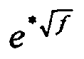
ou - lorsqu'on désigne l'atténuation en dB - sensiblement proportionnelle à la racine carrée de la fréquence
caractérisé par le fait que
le filtre (10) comprend une pluralité d'étages de filtre différents (300A, 300B, 300C; 400A, 400B, 400C) suivant substantiellement, chacun, une caractéristique d'atténuation caractérisée par des comportements asymptotiques pour des fréquences supérieures et pour des fréquences inférieures et un comportement de transition entre les deux comportements asymptotiques, les caractéristiques d'atténuation des différents étages de filtre (300A, 300B, 300C; 400A, 400B, 400C) se superposant, pour obtenir les caractéristiques d'atténuation du filtre (10).
ou - lorsqu'on désigne l'atténuation en dB - sensiblement proportionnelle à la racine carrée de la fréquence
caractérisé par le fait que
le filtre (10) comprend une pluralité d'étages de filtre différents (300A, 300B, 300C; 400A, 400B, 400C) suivant substantiellement, chacun, une caractéristique d'atténuation caractérisée par des comportements asymptotiques pour des fréquences supérieures et pour des fréquences inférieures et un comportement de transition entre les deux comportements asymptotiques, les caractéristiques d'atténuation des différents étages de filtre (300A, 300B, 300C; 400A, 400B, 400C) se superposant, pour obtenir les caractéristiques d'atténuation du filtre (10).
2. Filtre selon la revendication 1, dans lequel la pluralité d'étages de filtre (300A,
300B, 300C; 400A, 400B, 400C) sont conçus de sorte que les comportements de transition
soient répartis sur la plage de fréquences pertinente.
3. Filtre selon la revendication 2, dans lequel les fréquences centrales des étages (300A,
300B, 300C; 400A, 400B, 400C) sont réparties sur la plage de fréquences pertinente.
4. Filtre selon l'une des revendications 1 à 3, dans lequel la plage de fréquences pertinente
est divisée en une pluralité de sous-plages et chaque sous-plage sera dominée par
le comportement de transition d'un étage (300A, 300B, 300C; 400A, 400B, 400C).
5. Filtre selon l'une des revendications 1 à 4, dans lequel la pluralité d'étages de
filtre (300A, 300B, 300C; 400A, 400B, 400C) sont conçus de sorte que l'atténuation
d'étage augmente lorsque la fréquence centrale augmente.
6. Filtre selon l'une des revendications 1 à 5, dans lequel le filtre (10) comprend trois
étages de filtre (300A, 300B, 300C; 400A, 400B, 400C).
7. Filtre selon l'une des revendications 1 à 6, dans lequel le filtre (10) comprend une
pluralité d'étages (300A, 300B, 300C; 400A, 400B, 400C) ayant, chacun, le même aménagement
de composants ou schémas, mais avec des valeurs de composant différentes.
8. Filtre selon la revendication 7, dans lequel chaque étage (300A, 300B, 300C) comprend
deux résistances en série avec une troisième résistance couplée entre les deux résistances,
un condensateur couplé en parallèle aux deux résistances, et un inducteur connecté
en série à la troisième résistance, de préférence entre la troisième résistance et
la terre.
9. Filtre selon l'une des revendications 1 à 5, dans lequel le filtre (10) comprend deux
résistances en série, une troisième résistance couplée entre les deux résistances,
un inducteur connecté en série à la troisième résistance, un premier condensateur
en série avec une résistance couplée en parallèle aux deux résistances, et un deuxième
condensateur, avec ou sans résistance en série, couplé en parallèle aux deux résistances.
10. Filtre selon l'une des revendications 1 à 9, dans lequel la plage de fréquences pertinente
est de l'ordre de 1 MHz à 100 GHz et, de préférence, de l'ordre de 50 MHz à 20 GHz.
11. Dispositif de mesure adapté pour recevoir un signal de réponse (20), le signal de
réponse (20) étant dégradé par un trajet de transmission (30), comprenant un filtre
(10) selon l'une des revendications 1 à 10 pour compenser le signal de réponse dégradé
(40).
12. Matériel de test automatisé adapté pour fournir un signal de stimulus à un dispositif
à tester - DUT - et pour recevoir un signal de réponse (20) représentant la réponse
du DUT au signal de stimulus, dans lequel le signal de réponse (20) est dégradé par
un trajet de transmission (30), le matériel de test automatisé comprenant un filtre
(10) selon l'une des revendications 1 à 10 pour compenser le signal de réponse dégradé
(40).
REFERENCES CITED IN THE DESCRIPTION
This list of references cited by the applicant is for the reader's convenience only. It does not form part of the European patent document. Even though great care has been taken in compiling the references, errors or omissions cannot be excluded and the EPO disclaims all liability in this regard.
Patent documents cited in the description
- EP859318A [0002]
- EP864977A [0002]
- EP886214A [0002]
- EP882991A [0002]
- EP1092983A [0002]
- US5499248A [0002]
- US5453995A [0002]
- EP0467412A2 [0006]
- US4768205A [0007]
Non-patent literature cited in the description
- SAWAI ACOAXIAL PCM TRANSMISSION USING DUOBINARY SCHEMENEC Research and Development, 1981, 89-96 [0005]