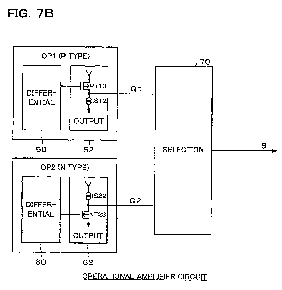
(57) In a period T1 (positive polarity) in which a voltage level of a counter electrode
VCOM becomes VC1, a data line is driven using P-type operational amplifier OP1 having
P-type driving transistor, while in a period T2 (negative polarity) in which VCOM
becomes VC2, the data line is driven using N-type operational amplifier OP2 having
N-type driving transistor. An output of a selection circuit for the operational amplifiers
OP1, OP2 is set to the high impedance state when VCOM is changed over. At the time
of driving the operational amplifier OP1, a current which flows in current sources
of the operational amplifier OP2 is cut off, while at the time of driving the operational
amplifier OP2, a current which flows in current sources of the operational amplifier
OP1 is cut off. In the period before the operational amplifiers OP1, OP2 are driven,
the driving transistors of the operational amplifiers OP1, OP2 are turned off. The
voltage level of the data line can be changed before driving by positively utilizing
the parasitic capacitance between the counter electrode and data line.
|
|
