(57) A passive device and module for a transceiver, and a manufacturing method thereof
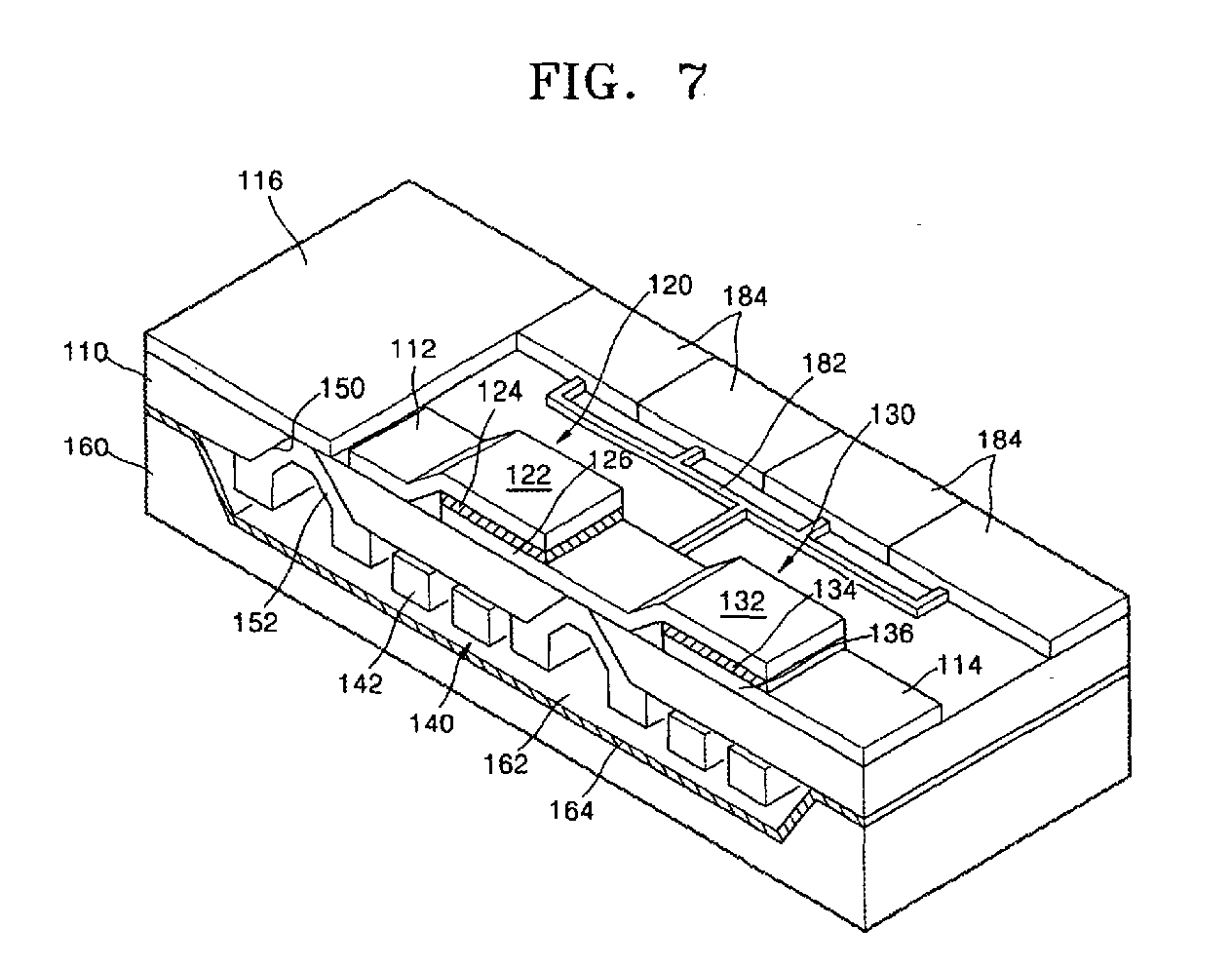
are provided. The passive device includes a semiconductor or a dielectric substrate,
at least one capacitor, at least one inductor, a viahole, a metal electrode, radio
frequency signals, a radio frequency ground, a packaging substrate. The capacitor
is formed on a first surface of the substrate. The inductor is formed on a second
surface of the substrate that is opposite to the first surface. The viahole penetrates
through the substrate. The metal electrode is formed on the viahole and electrically
connects the capacitor on the first surface and the inductor on the second surface.
The radio frequency ground is formed on the substrate and isolated from the radio
frequency signals. The packaging substrate is bonded on the substrate, having a cavity
covering a structure on the bonded surface of the substrate. Also, use of MEMS technique
can reduce insertion loss of inductors, which improves the communication quality of
the communication systems.
|
|
