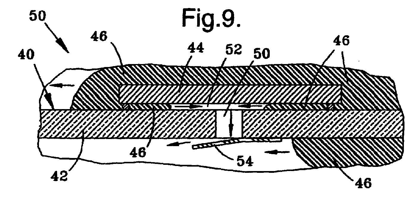
(57) An overmolded circuit board assembly (30,50) and a method for forming the assembly
(30,50). The assembly (30,50) and method entail overmolding both surfaces of a circuit
board (12,42,62,82) and underfilling at least one surface-mount circuit device (14,44,64,84)
attached to at least one surface of the board (12,42,62,82) with solder bump connections
(18,48), with the result that the circuit device (14,44,64,84) is spaced above the
surface of the circuit board (12,42,62,82) so as to define a gap (22,52,72,92) therebetween.
The circuit board assembly (30,50) further comprises a cavity (20,50,70,90), such
as a blind hole (30) or closed through-hole (50,70,90), defined in the surface of
the circuit board (12,42,62,82) beneath the circuit device (14,44,64,84), such that
the cavity (20,50,70,90) communicates with the gap (22,52,72,92) between the circuit
board (12,42,62,82) and device (14,44,64,84), but is closed off from the opposite
surface of the circuit board (12,42,62,82). As a result of the presence of the cavity
(20,50,70,90), air that becomes trapped in the gap (22,52,72,92) by a molding material
(16,46) during the overmolding/underfilling process is collected and compressed within
the cavity (20,50,70,90), yielding a void-free underfill between the circuit board
(12,42,62,82) and
|
|
