(19)
(11) EP 1 317 002 A3

(12) EUROPEAN PATENT APPLICATION

(88) Date of publication A3:
29.09.2004 Bulletin 2004/40

(43) Date of publication A2:
04.06.2003 Bulletin 2003/23

(21) Application number: 02090384.5

(22) Date of filing: 20.11.2002
(51) International Patent Classification (IPC)7: H01L 29/786
(84) Designated Contracting States:
AT BE BG CH CY CZ DE DK EE ES FI FR GB GR IE IT LI LU MC NL PT SE SK TR
Designated Extension States:
AL LT LV MK RO SI

(30) Priority: 27.11.2001 KR 2001074375

(71) Applicant: Samsung SDI Co. Ltd.
Suwon-city, Kyonggi-do (KR)

(72) Inventor:
  • Lee, Ki-Yong
    Yongin-city (KR)

(74) Representative: Ziebig, Marlene, Dr. Dipl.-Chem. et al
Anwaltskanzlei Gulde Hengelhaupt Ziebig & Schneider Wallstrasse 58/59
10179 Berlin
10179 Berlin (DE)


(54) Poly-silicon layer of a thin film transistor and display device having the same


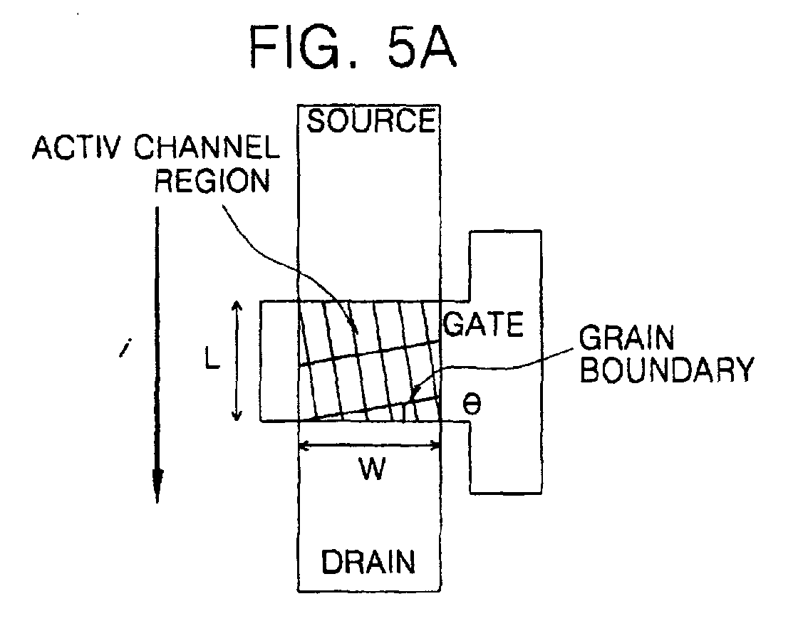
(57) A poly-silicon layer of a thin film transistor (TFT) having an active channel region, wherein a probability P that a maximum number of a primary grain boundary exists on the active channel region is not 0.5, the probability obtained by the following equation:P = D - (N max - 1) · GsGs    , where D = L·cosθ +W·sinθ, L is a channel length of the active channel region, W is a width of the active channel region, Nmax is the maximum number of the primary boundary existing on the active channel region, Gs is a grain size, and θ is a tilt angle of the primary grain boundary and the display device having thereof.


Search report