(19)
(11) EP 1 321 987 A3

(12) EUROPEAN PATENT APPLICATION

(88) Date of publication A3:
01.12.2004 Bulletin 2004/49

(43) Date of publication A2:
25.06.2003 Bulletin 2003/26

(21) Application number: 02258796.8

(22) Date of filing: 19.12.2002
(51) International Patent Classification (IPC)7H01L 41/187, H01L 41/24
(84) Designated Contracting States:
AT BE BG CH CY CZ DE DK EE ES FI FR GB GR IE IT LI LU MC NL PT SE SI SK TR
Designated Extension States:
AL LT LV MK RO

(30) Priority: 20.12.2001 JP 2001388315

(71) Applicant: NGK INSULATORS, LTD.
Nagoya-City, Aichi Prefecture 467-8530 (JP)

(72) Inventors:
  • Kashiwaya, Toshikatsu, IPD NGK Insulators, Ltd.
    Nagoya-shi, Aichi-ken 467-8530 (JP)
  • Kitagawa, Mutsumi, IPD NGK Insulators, Ltd.
    Nagoya-shi, Aichi-ken 467-8530 (JP)

(74) Representative: Paget, Hugh Charles Edward et al
Mewburn Ellis LLP York House 23 Kingsway
London WC2B 6HP
London WC2B 6HP (GB)


(54) Piezoelectric element and process for production thereof


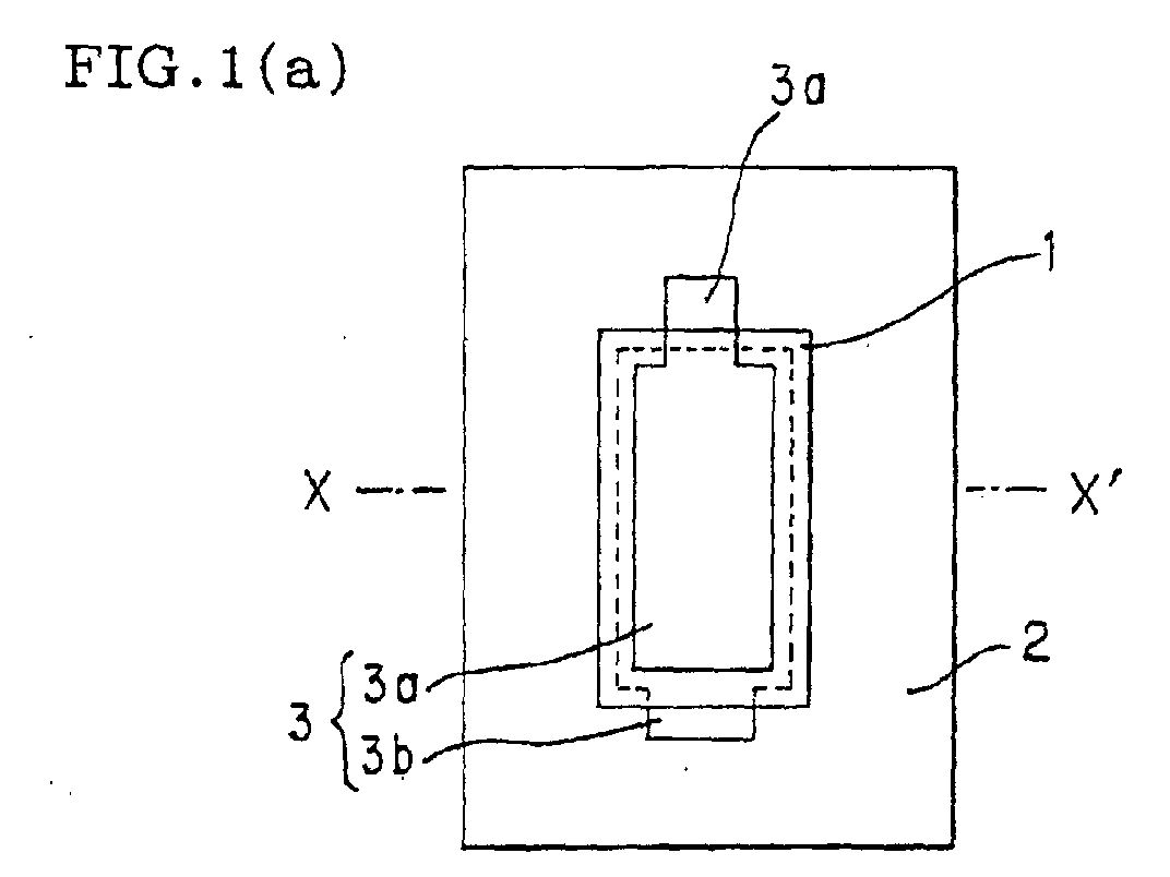
(57) A piezoelectric element includes: a ceramic substrate (2), a piezoelectric portion (1) made of a piezoelectric ceramic composition containing a Pb(Mg, Ni)1/3Nb2/3O3-PbZrO3-PbTiO3 ternary system solid solution composition being represented by the following general formula (1) as a main component, and an electrode (3). The electrode is electrically connected to the piezoelectric portion, and the piezoelectric portion is solidly attached to the ceramic substrate directly or via the electrode.Pbx{(Mg1-yNiy)1/3×aNb2/3}bTicZrdO3 wherein 0.95≦x≦1.05; 0.05≦y≦0.20; 0.90≦a≦1.10; b, c and d are decimals falling in a range surrounded by (b,c,d) = (0.550,0.425,0.025), (0.550,0.325,0.125), (0.375,0.325,0.300), (0.100,0.425,0.475), (0.100,0.475,0.425) and (0.375,0.425,0.200) in the coordinates with coordinate axes of said b, c and d, and b+c+d = 1.000.


Search report