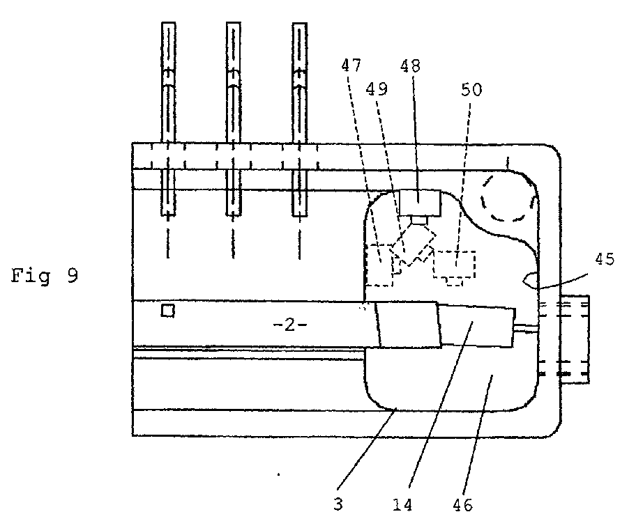
(57) An active optical device, preferably a Mach Zehnder modulator, comprises a packaged
optical chip (2,3), an optical fibre (13) coupled to the chip (2) to receive an optical
output from it, and a photodetector (15) located within the package for receiving
part of the radiation light (11) for monitoring the amplitude of that optical output.
Said part of the radiation light (11,12) corresponds to the light that is produced
by destructive interference in a pair of waveguides (21,22,9) that merge together
at a small angle chosen such that a substantial part of the light (ideally nearly
all of it) propagates through the substrate of the chip in only two directions (corresponding
to a first-order diffraction (11,12)). The optical fibre (13) is coupled to the chip
by means of a fibre support (14) (such as a fibre block or a ferrule) made of transparent
material, and the photodetector (15) is positioned to receive the radiation light
(11) at least partly through the fibre support and at least partly by reflection from
the interior of the package.
Using light that passes through the fibre support in this way overcomes the apparent
problem that the radiation light emitted in the first-order diffraction lobes is too
close to the output waveguide (10,23).
When the device comprises an attenuator and a modulator, the photodiode can serve
at the same time to control the bias setting of the modulator and the output power
level determined by the attenuator setting.
|
|
