(57) The present invention easily achieves an accurate control structure for limiting
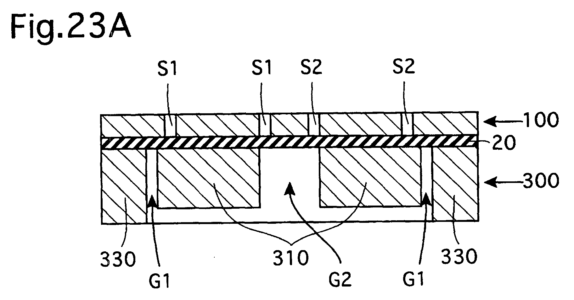
displacement of a weight (310; 310B). An SOI substrate with a trilaminar structure
including a silicon layer (10), a silicon oxide layer (20), and a silicon layer (30)
is prepared, and slits (S1-S4) are opened by applying induced coupling plasma etching
which can selectively remove only silicon from the upper side. Then, the same etching
is applied from the lower side to form grooves (G1, G2), whereby the silicon layer
(30) is separated into a weight (310; 310B) and a pedestal (330; 330B). Next, the
structure is immersed in an etchant which can selectively remove only silicon oxide,
whereby the vicinities of exposed portions of the silicon oxide layer (20) are removed
to form joint layers. A glass substrate (400) is joined to the bottom surface of the
pedestal (330; 330B). Piezo resistor elements (Rx1-Rx4, Ry1-Ry4, Rz1-Rz4) are formed
on the upper surface of the silicon layer (100) to detect bending. The degree of freedom
of upward displacements of the weight (310; 310B) is accurately set based on the thickness
of the joint layer (200; 200B).
|
|
