(19)
(11) EP 1 394 945 A3

(12) EUROPEAN PATENT APPLICATION

(88) Date of publication A3:
10.03.2004 Bulletin 2004/11

(43) Date of publication A2:
03.03.2004 Bulletin 2004/10

(21) Application number: 03090254.8

(22) Date of filing: 07.08.2003
(51) International Patent Classification (IPC)7H03K 17/10, H03K 17/0412, H03K 17/284
(84) Designated Contracting States:
AT BE BG CH CY CZ DE DK EE ES FI FR GB GR HU IE IT LI LU MC NL PT RO SE SI SK TR
Designated Extension States:
AL LT LV MK

(30) Priority: 07.08.2002 JP 2002230452

(71) Applicant: Nippon Telegraph and Telephone Corporation
Tokyo 100-8116 (JP)

(72) Inventors:
  • Yohtaro, Umeda NTT Intellectual Property Center
    Musashino-shi Tokyo 180-8585 (JP)
  • Atsushi, Kanda NTT Intellectual Property Center
    Musashino-shi Tokyo 180-8585 (JP)

(74) Representative: Patentanwälte Wenzel & Kalkoff 
Grubesallee 26
22143 Hamburg
22143 Hamburg (DE)


(54) Driver circuit


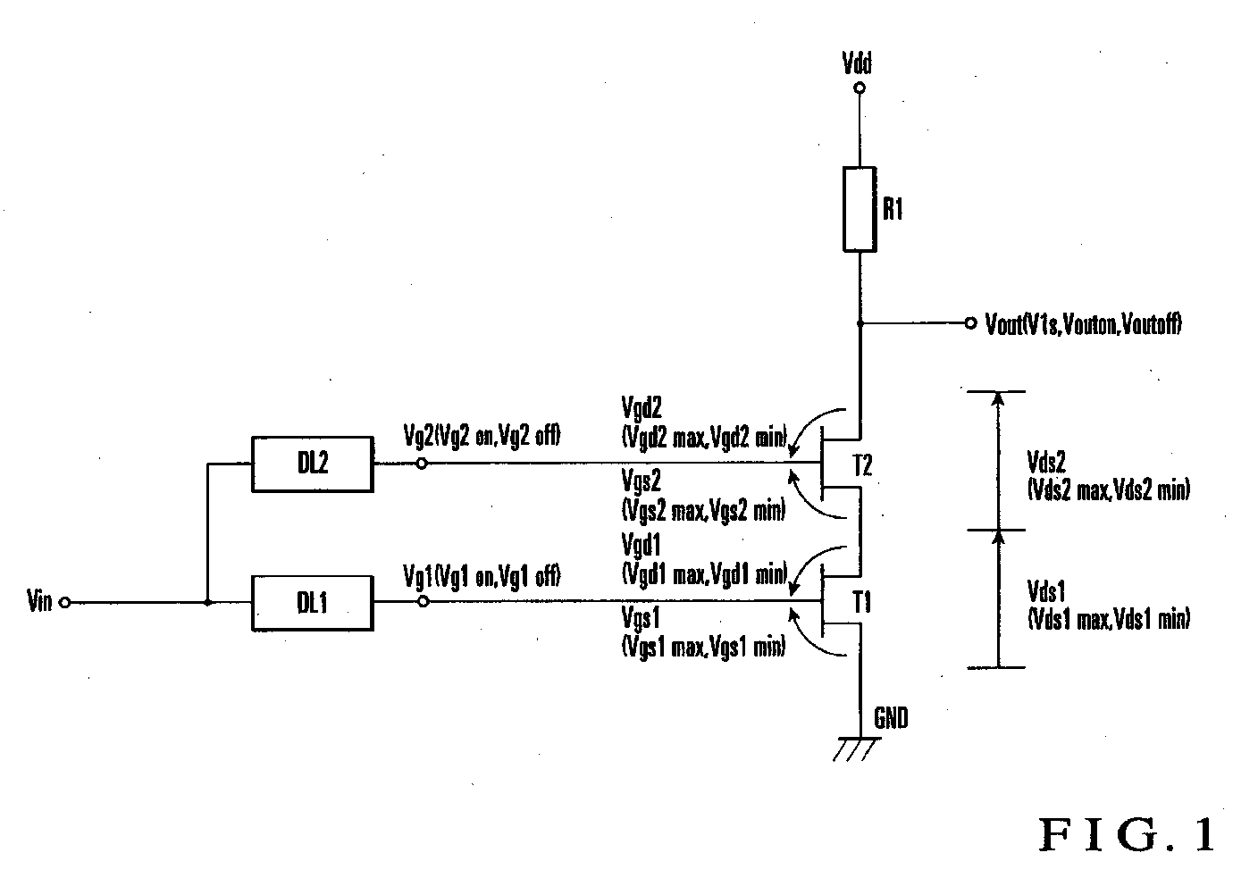
(57) A driver circuit includes first (T1) and second (T2) three-terminal active elements, and first (DL1) and second (DL2) delay units. The first and second three-terminal active elements (T1,T2) are series-connected. Each of the first and second three-terminal active elements (T1,T2) has an amplification function and first, second, and third electrodes. The second and third electrodes of each three-terminal active element (T1,T2) are series-connected between the first and second potentials (Vdd,GND). The first and second delay units (DL1,DL2) receive the same input signal (Vin). The outputs of the first and second delay units (DL1,DL2) are respectively connected to the first electrodes of the first and second three-terminal active elements (T1,T2). The delay amount of the second delay unit (DL2) is larger than that of the first delay unit (DL1). The delay amount of the first delay unit (DL1) is a finite value including zero.


Search report