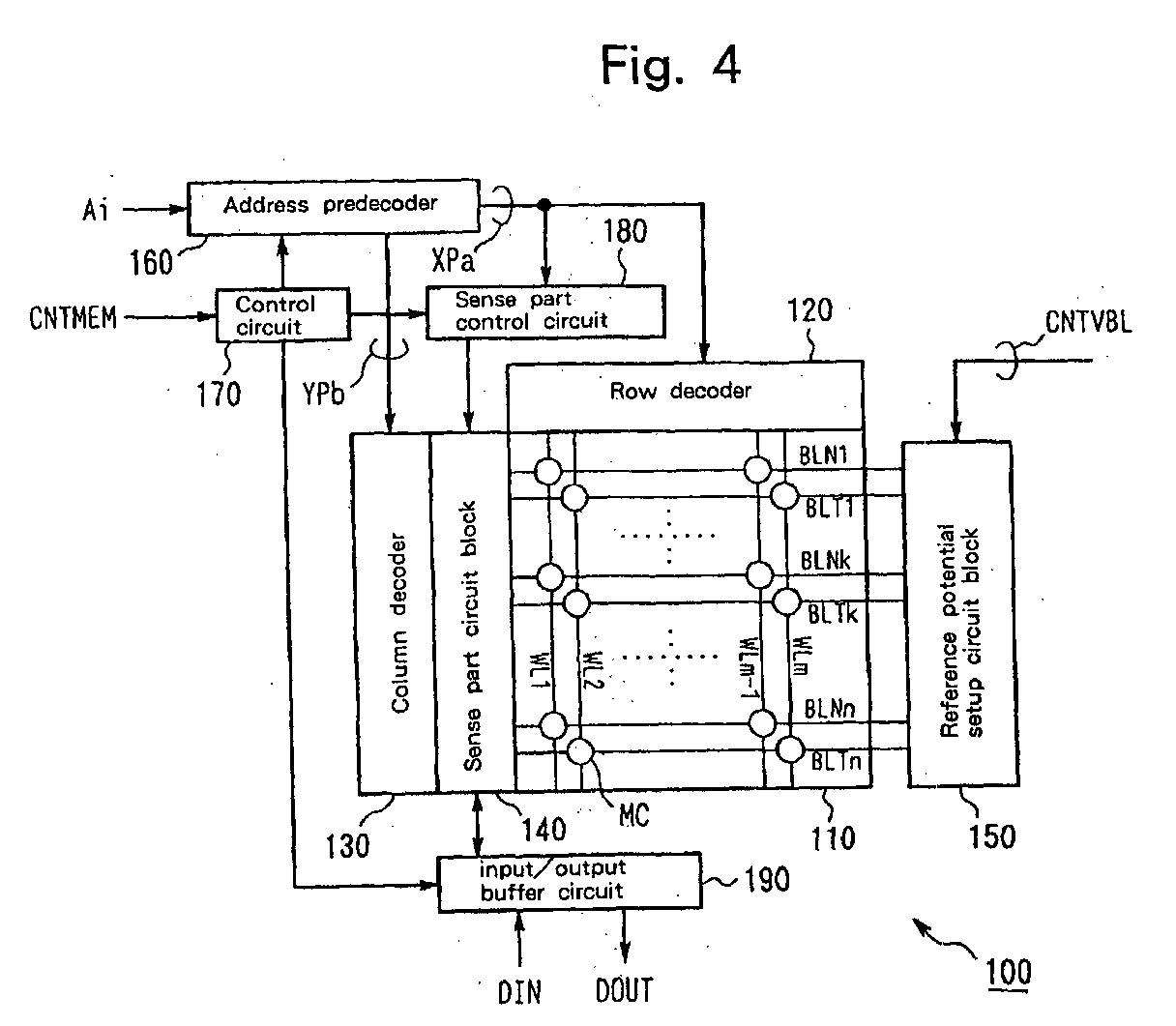
(57) The object of the present invention is to provide a semiconductor memory device wherein
analog data signal potential read out from a memory cell to bit-line (bit-line read-out
potential) can be measured precisely. In this invention, a sense part circuit block
140 differentially amplifies data signal occurring on one of a pair of bit-lines (for
example, bit-line BLNk, BLTk) in a memory cell array 110, and reference signal occurring
on another of the pair, and data is read out. Bit-lines BLN1, BLT1, -, BLNn, BLTn
are connected to a reference potential setup circuit block 150. Reference potential
setup circuit 150 sets up potential assigned from outside of the device as potential
of reference signal on bit-line. Bit-line read-out potential is indirectly obtained
from the differential amplification result by controlling the reference potential
with the reference potential setup circuit block 150.
|
|
