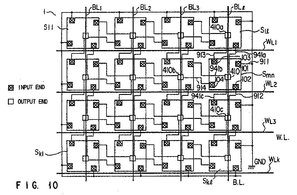
(57) A semiconductor memory device, comprising:
- a plurality of bit lines (BL),
- a plurality of word lines (WLk), and
- first and second memory structure units provided at a cross-position between the bit
lines and the word lines,
- wherein each of the first and second memory structure units comprises:input means
(100) input with first data from outside,operation means (200) for operating first
data input from the input means (100) to generate second data,memory means (300) for
storing the second data,
- output means (400) for outputting the second data stored in the memory means (300)
to the outside,
- control means (500) for controlling the memory means (300) to enable storing and outputting
of the second data,switch means (2312) in which connection and disconnection between
the memory means (300) and a bit line are controlled by a word line, andconnecting
means (911,912,913,914) for electrically connecting the input means of the first memory
structure unit and the output means of the second memory structure unit with each
other.
|
|
