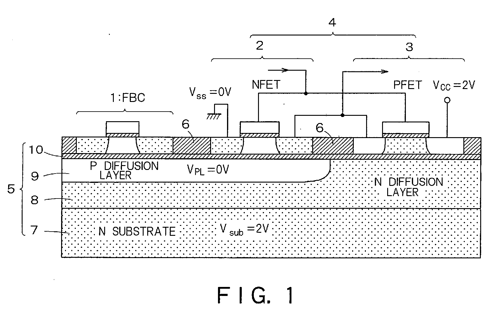
(57) A semiconductor storage device according to the present invention, comprising: a
first semiconductor layer formed on a substrate via a buried insulation layer; an
FBC (Floating Body Cell) having a channel body of floating type formed on the first
semiconductor layer, a main gate which forms a channel at a first face side of the
channel body, and an auxiliary gate formed to capacitively couple on a second face
at an opposite side of the first face; a logic circuit formed on the first semiconductor
layer, separate from the FBC by an insulation film, which transfers a signal for the
FBC; a second semiconductor layer which locates below the FBC and is formed along
an under face of the buried insulation film; and a third semiconductor layer which
locates below the logic circuit and is formed along an under face of the buried insulation
film, wherein the second and third semiconductor layers are set to be in a potential
different from each other.
|
|
