|
(11) | EP 1 612 949 A1 |

| (12) | EUROPEAN PATENT APPLICATION |
|
|
|
|
||||||||||||||||||||
| (54) | Method and system for correcting errors in electronic memory devices |
| (57) The invention relates to a method and system for correcting errors in multilevel
memories using binary BCH codes. The number of errors is estimated by analyzing the
syndrome components (5). If the number of estimated errors is one, then simple decoding
for a Hamming code is performed. Otherwise, conventional decoding of the BCH code
is carried out (2,3). This avoids the computation of the error locator polynomial
and its roots in the presence of only one error and, thus, reduces the average decoding
complexity.
|
Field of application
[0001] The present invention relates to a method and system for correcting errors in electronic memory devices, for example read and write non volatile memories, particularly Flash electronic memories.
[0002] The invention particularly relates to read and write memories having a NAND structure and the following description is made with reference to this specific field of application for convenience of illustration only, since the invention can be also applied to memories with NOR structure, provided that they are equipped with an error correction system.
[0003] Even more particularly, the invention relates to a method and system for correcting errors in electronic read and write non volatile memory devices, particularly Flash memories, of the type providing the use of a BCH binary correction code.
Prior art
[0004] As it is well known in this specific technical field, two-level and multilevel NAND memories have such a Bit Error Rate (BER) as to require an Error Correction system (ECC) in order to allow them to be used as much reliably as possible.
[0005] Among the innumerable present correction systems ECC a particular importance is assumed by the so-called cyclical correction codes, particularly BCH binary codes.
[0007] This code operates on a block of binary symbols. If N (4096 + 128) is the block size, the number of parity bits is P (52bit).
[0008] The canonical coding and decoding structures process the data block by means of sequential operations on the bits to be coded or decoded.
[0009] The arithmetic operators (sum, multiplication, inversion) in GF(2) are extremely simple (XOR, AND, NOT).
[0011] For a better understanding of all the aspects of the present invention, the structure of the error correction systems using a BCH code will be analysed hereafter.
The BCH structure
[0012] The typical structure of a BCH code is shown in the attached figure 1 wherein the block indicated with C represents the coding step while the other blocks 1, 2 and 3 are active during the decoding and they refer to the syndrome calculation, to the error detection polynomial calculation (for example by means of the Berlekamp algorithm) and to the error detection, respectively. The block M indicates a storage and/or transfer medium of the coded data.
[0013] It is worth realising blocks C, 1 and 3 by means of known sequential structures, (for example as described by: Shu Lin, Daniel Costello - in: "Error Control Coding: Fundamentals and Applications") having a latency being proportional to the length of the message to be stored.
[0014] In particular for a traditional sequential implementation:
BLOCK C: the block latency is equal to the message to be stored (4096 bits);
BLOCK 1: the block latency is equal to the coded message (for a four-error-corrector code 4096+52);
BLOCK 3: the block latency is equal to the coded message (for a four-error-corrector code 4096+52).
[0015] By means of traditional implementations of the coding block C and syndrome calculation block 1, the latency time used for these operations can be partially or totally overlapped respectively to the information writing time in the memory and to the data reading time (without any correction) by the user. These coding and decoding steps can thus not require an increase in the time required for reading and writing. At the end of the information block reading (N bits), the block 1 has calculated the syndromes. If all the syndromes are equal to 0, it is not necessary to perform other operations. If the syndromes are not equal to 0, the decoding steps 2 and 3 are to be performed. The impact on the system performances given by the performance of these two steps (2 and 3), however they are implemented, is much higher the more the packages with one or more errors are frequent.
[0016] Although advantageous under several aspects, known systems do not allow the frequency of use of decoding blocks 2 and 3 to be reduced yet, which would allow to reduce the decoding complexity.
[0017] The technical problem underlying the present invention is to provide an error correction method and system allowing the decoding step burden to be reduced, overcoming the drawbacks of the solutions provided by the prior art.
Summary of the invention
[0018] The solution idea underlying the invention is to decrease the frequency of use of decoding blocks 2 and 3 by using the binary properties of BCH correction codes, particularly a relation on the syndromes.
[0019] It is thus possible to optimise the system speed by recognising when a single error occurred and by using for this case a Hamming decoding.
[0020] On the basis of this solution idea, the technical problem is solved by a system as previously indicated and defined in claim 1.
[0022] The features and advantages of the system and method according to the invention will be apparent from the following description of an embodiment thereof given by way of non limiting example with reference to the attached drawings.
Brief description of the drawings
[0024]
- Figure 1 is a schematic block view of a BCH coding and decoding system;
- Figure 2 is a schematic block view of a BCH coding and decoding system emphasising the blocks being concerned only in case of error;
- Figure 3 shows in a diagram a comparison between the error probabilities in two-level memories and in multilevel memories;
- Figure 4 is a schematic block view of a coding and decoding system according to the present invention;
- Figure 5 shows in a diagram a comparison between the error probabilities in two-level memories and in multilevel memories according to the method of the present invention by indicating the frequency of use of the heaviest decoding blocks.
Detailed description
[0025] With reference to the drawings of the attached figures, and particularly to the example of figure 2, an error correction system for electronic non volatile memory devices, particularly multilevel reading and writing memories, is globally and schematically indicated with 10.
[0026] The system 10 comprises a block indicated with C representing the coding step; a block M indicating the electronic memory device and a group of blocks 1, 2 and 3 which are active during the decoding step. In particular, the block 1 is responsible for calculating the so-called code syndrome, the block 2 is a calculation block of the error detector polynomial, while the block 3 is responsible for detecting the error by means of the Chien wrong position search algorithm.
[0027] The BCH decoding requires the syndrome calculation, block 1. This calculation can occur while the user reads data from the memory and therefore it can not involve a time over-head.
[0028] If all the calculated syndromes are equal to zero, the data package being read is correct or the number of errors is higher than 2K, where K indicates the code corrective capacity. If not all the syndromes are null, it is necessary to proceed with the decoding steps 2 and 3. These steps, however implemented, involve a time over-head for the implementation thereof.
[0029] The impact of this over-head on the system performances is much higher the highest the frequency at which errors occur is.
[0030] Figure 3 emphasises, by way of example, the error probabilities of a block of 4096 bits for EEPROM Flash memories comprising 1bit/cell and 2bits/cell according to the single bit error probability. The frequency at which blocks 2 and 3 must intervene in the case of multilevel memories is 1 out of 50.
[0031] The invention is particularly suitable for the use in Flash EEPROM memories having a NAND structure; nevertheless nothing prevents the invention from being also applied to memories with NOR structure or memories of different type, provided that they are equipped with an error correction system.
[0032] Advantageously, the system according to the invention is based on a combination between a BCH code and a Hamming code in order to obtain a decoding step with a reduced use of decoding blocks 2 and 3.
[0033] The mathematical basics whereon the BCH and Hamming combination of the invention is based will be described hereafter.
[0037] In order to reduce the decoding over-head due to the implementation of steps 2 and 3, a relation between the wrong message syndromes has been searched for in order to recognise when a single error occurred and apply in this case a Hamming decoding.
[0038] In substance, the invention being shown in figure 4 provides a preventive control step of the need to correct a single error and a subsequent intervention demand of the system portion implementing the Hamming decoding, block 5 in figure 4.
[0039] Therefore the correction frequency using blocks 2 and 3 of the structure 10 drastically decreases. As exemplified in figure 5 in the case of 2bits/cell Flash memories, an intervention frequency of blocks 2 and 3 being equal to 1 out of 50 turns into an intervention frequency of blocks 2 and 3 being equal to 1 out of 1000.
[0040] Advantageously, the preventive control step is entrusted to the so-called decoding method "syndromes", i.e. to the block 1.
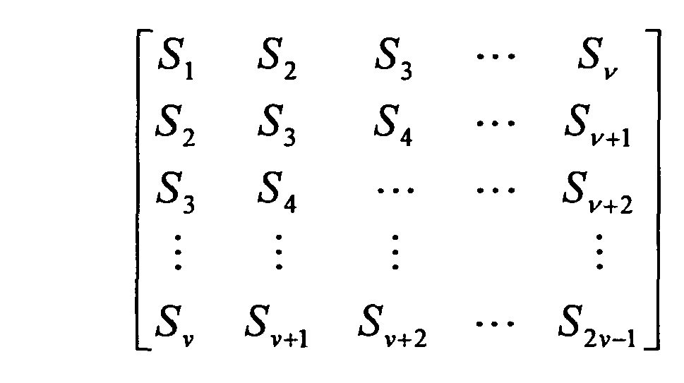
[0042] A matrix relation is now drawn, allowing to recognise from the syndromes calculated from the block 1 if a single error occurred:
[0043] In this case all the matrix determinants must be cancelled by setting ν = t, ν = t-1,..., ν = 2 (t indicates the code correction capacity). Only S1 must be different from zero.
[0045] It is worth remembering that in the case of a single error a Hamming code is used. This means that the syndrome S 1 univocally identifies the wrong position.
[0046] In fact the primitive element power corresponding to the obtained syndrome S1, represents the wrong position. If for example the obtained syndrome is the binary expression of the element α12 then the twelfth position is the wrong one.
[0047] The block 5 of figure 4 comprises means for identifying the relations between the above-mentioned syndromes and, if they are met, for obtaining from the syndrome S1 the error position. These means known in literature can be specific for correcting a single error in order to rapidly play the role thereof.
[0048] A particular exemplifying case is represented by a combinatory logic identifying the relations between the syndromes and a ROM memory translating the syndromes into the corresponding error positions.
[0049] The situation can be summed up by saying that all the possible syndromes have an associated error configuration and according to the present invention a BCH correction (block 2 and 3) is used only when two or more errors occurred.
[0050] The general system structure according to the invention is shown in figure 4 and it clearly shows the presence of an analysis block 5 connected to the output of the block 1 responsible for the syndrome calculation step.
[0051] The output of the block 5 is directly transferred into an adder node 6 wherein also the output of the error detection block 3 converges.
[0052] Therefore when the system 10 detects the presence of a single error, the control is entrusted to a Hamming code decoding correcting only that error.
[0054] Consequently the speed increases since blocks 2 and 3, being structurally more complex, are used rarely with respect to known solutions.
[0055] This advantage is well shown in the diagram of figure 5 wherefrom it can be recognised how the error probability is different for single errors and for multiple errors, making the use of the method and system according to the present invention very profitable.
[0056] The method according to the invention thus provides the alternative use of a Hamming correction code at each detection of a single error to be corrected.
1. A method for correcting errors in electronic memory devices providing the use of a
BCH binary error correction code, characterised in that it comprises the alternative use of a Hamming correction code at each detection of
a single error to be corrected.
2. A method according to claim 1, characterised in that the detection of a single error is obtained by analysing the result of the syndrome
calculation step.
3. A method according to claim 2, characterised in that the recognition by the syndromes of the presence of a single error is based on the
following matrix relation:
putting equal to zero all the matrix determinants which are obtained by setting ν = 2, ..., t wherein t indicates the code correction capacity and only with S1 different from zero.
putting equal to zero all the matrix determinants which are obtained by setting ν = 2, ..., t wherein t indicates the code correction capacity and only with S1 different from zero.
4. A method according to claim 3, characterised in that, by means of said matrix and by using the binary property S2i = Si2, the following relations are obtained:

5. A system for correcting errors in memory electronic devices, providing the use of
a coding block (C) with a BCH binary correction code and a cascade of decoding blocks
(1, 2, 3) wherein a first block (1) is responsible for calculating the code syndrome,
a second block (2) for calculating the error detector polynomial and a third block
(3) responsible for detecting the error, characterised in that it comprises a block (5) for analysing the syndrome and detecting single errors,
connected to the output of the first block (1) to detect the presence of single errors.
6. A system according to claim 5, characterised in that the output of said analysis and detection block (5) is directly transferred in an
adder node (6) wherein also the output of the third error detection block (3) converges,
reducing the decoding time in case of single error.
7. A system according to claim 5, characterised in that the output of said analysis block (5) bypasses said second and third block (3), whose
frequency of use is considerably reduced.
8. A system according to claim 5, characterised in that said electronic memory devices are multilevel memories.