(19)
(11) EP 0 849 878 A3

(12) EUROPEAN PATENT APPLICATION

(88) Date of publication A3:
26.06.2002 Bulletin 2002/26

(43) Date of publication A2:
24.06.1998 Bulletin 1998/26

(21) Application number: 97310290.8

(22) Date of filing: 18.12.1997
(51) International Patent Classification (IPC)7H03H 11/46, H03H 11/24
(84) Designated Contracting States:
AT BE CH DE DK ES FI FR GB GR IE IT LI LU MC NL PT SE
Designated Extension States:
AL LT LV MK RO SI

(30) Priority: 19.12.1996 US 33478 P

(71) Applicant: TEXAS INSTRUMENTS INCORPORATED
Dallas Texas 75265 (US)

(72) Inventors:
  • Zhang, Zhengwei
    Richardson, TX 75081 (US)
  • Hellums, James R.
    Plano, TX 75093 (US)

(74) Representative: Legg, Cyrus James Grahame et al
ABEL & IMRAY, 20 Red Lion Street
London WC1R 4PQ
London WC1R 4PQ (GB)


(54) Improvements in or relating to integrated circuits


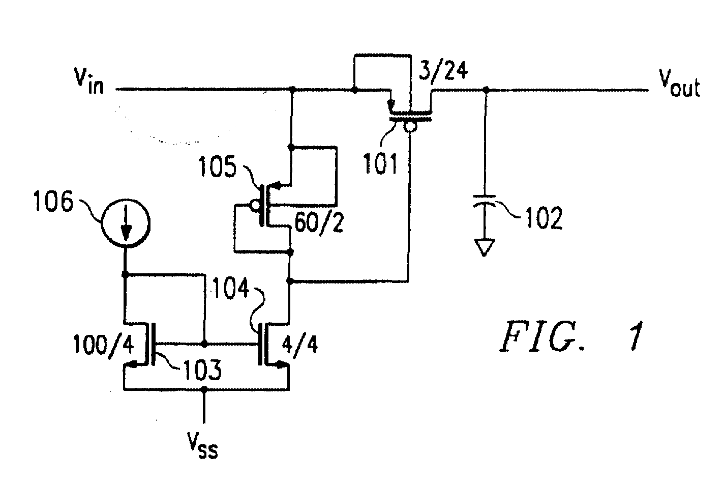
(57) A resistive element including a P-channel MOS device (101, 401, 402, 608a-608c) having a first and second current carrying electrodes, and a gate. The first current carrying electrode forms a first impedance terminal and the second current carrying electrode forms a second impedance terminal. A bias circuit (103, 104, 105, 106) coupled to the first current carrying electrode and gate of the P-channel MOS device (101, 401, 402, 608a-608c). The bias circuit (103, 104, 105, 106) generates a voltage less than the threshold voltage of the P-channel MOS device (101, 401, 402, 608a-608c).


Search report